7 www.national.com
CP3BT26
3.21 POWER MANAGEMENT
The Power Management Module (PMM) improves the effi-
ciency of the device by changing the operating mode and
power consumption to match the required level of activity.
The device can operate in any of four power modes:
— Active: The device operates at full speed using the
high-frequency clock. All device functions are fully op-
erational.
— Power Save: The device operates at reduced speed
using the Slow Clock. The CPU and some modules
can continue to operate at this low speed.
— Idle: The device is inactive except for the Power Man-
agement Module and Timing and Watchdog Module,
which continue to operate using the Slow Clock.
— Halt: The device is inactive but still retains its internal
state (RAM and register contents).
3.22 DMA CONTROLLER
The Direct Memory Access Controller (DMAC) can speed
up data transfer between memory and I/O devices or be-
tween two memories, relative to data transfers performed di-
rectly by the CPU. A method called cycle-stealing allows the
CPU and the DMAC to share the CPU bus efficiently. The
DMAC implements four independent DMA channels. DMA
requests from a primary and a secondary source are recog-
nized for each DMA channel, as well as a software DMA re-
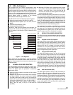
quest issued directly by the CPU. Table 1 shows the DMA
channel assignment on the CP3BT26 architecture. The fol-
lowing on-chip modules can assert a DMA request to the
DMAC:
• CR16C (Software DMA request)
•USB
• USART
• Advanced Audio Interface
• CVSD/PCM Converter
Table 1 shows how the four DMA channels are assigned
to the modules listed above.
Table 1 DMA Channel Assignment
The interface can handle data words of either 8- or 16-bit
length and data frames can consist of up to four slots.
In the normal mode of operation, the interface only transfers
one word at a periodic rate. In the network mode, the inter-
face transfers multiple words at a periodic rate. The periodic
rate is also called a data frame and each word within one
frame is called a slot. The beginning of each new data frame
is marked by the frame sync signal.
3.23 SERIAL DEBUG INTERFACE
The Serial Debug Interface module (SDI module) provides
a JTAG-based serial link to an external debugger, for exam-
ple running on a PC. In addition, the SDI module integrates
an on-chip debug module, which allows the user to set up to
eight hardware breakpoints on instruction execution and
data transfer. The SDI module can act as a CPU bus master
to access all memory mapped resources, such as RAM and
peripherals. Therefore it also allows for fast program code
download into the on-chip Flash program memory using the
JTAG interface.
3.24 DEVELOPMENT SUPPORT
In addition to providing the features needed for the next gen-
eration of embedded Bluetooth products, the CP3BT26 de-
vices are backed up by the software resources designers
need for rapid product development, including an operating
system, Bluetooth protocol stack implementation, peripher-
al drivers, reference designs, and an integrated develop-
ment environment. Combined with National’s LMX5251
Bluetooth radio transceiver, the CP3BT26 devices provide a
total Bluetooth system solution.
National Semiconductor offers a complete and industry-
proven application development environment for CP3BT26
applications, including the IAR Embedded Workbench,
iSYSTEM winIDEA and iC3000 Active Emulator, Bluetooth
Development Board, Bluetooth Protocol Stack, and Applica-
tion Software. See your National Semiconductor sales rep-
resentative for current information on availability and
features of emulation equipment and evaluation boards.
Channel
Primary/
Secondary
Peripheral Transaction
0
Primary USB Read/Write
Secondary UART0 Read
1
Primary UART0 Write
Secondary Unused N/A
2
Primary AAI Read
Secondary CVSD/PCM Read
3
Primary AAI Write
Secondary CVSD/PCM Write


