www.national.com 276
CP3BT26
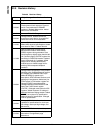
32.0 Revision History
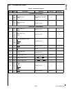
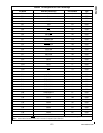
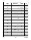
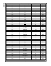
Table 96 Revision History
Date Major Changes From Previous Version
4/3/03 Original release.
5/26/03
Fixed maximum boot area in Section 8.
Fixed names of clock signals in Figures 5
and 6. Fixed addresses of FSMARx
registers in Register Map section. Added
default value for RNGDIV.
6/16/03 Corrected Table 27. Changed I
OH
and I
OL
.
6/30/03
Changed NSIDs, deleted commercial
temperature range device, changed ADC
conversion time to 15 microseconds.
10/7/03
Updated DC electrical specifications.
Added ADC electrical specifications. Added
more detail to Table 7. Added Table 25.
11/14/03
Defined valid range of SCDV field in
Microwire/SPI module. Noted default
PRSSC register value generates a Slow
Clock frequency slightly higher than 32768
Hz. Clarified usage of CVSTAT register bits
and fields in CVSD/PCM module. Updated
layout of Bluetooth LLC registers. Added
usage hint for avoiding ACCESS.bus
module bus error. Added usage hint for
avoiding CAN unexpected loopback
condition.
2/28/04
Changed NSID designations in the product
selection guide. Updated Bluetooth section
for LMX5251 and LMX5252 radio chips.
Added BTSEQ[3:1] signals to pin
descriptions, GPIO alternate functions, and
package pin assignments. Added entry for
CTIM register in CAN section register list.
Changed CVSD Conversion section.
Changed definition of the RESOLUTION
field of the CVSD Control register
(CVCTRL). Changed reset values for ADC
registers. Added maximum I/O voltage in
Absolute Maximum Ratings section. Added
RESET
Low minimum DC specification.
Added Iccprog DC specification. Changed
Vxl2 DC specification.
3/16/04
Changed LMX5251 interface circuit.
Updated DC specifications for clock input
low voltage, reset input high voltage, and
halt current.
5/10/04 Corrected NSIDs for no-lead solder parts.
5/12/04
Moved revision history in front of physical
dimensions. Changed back page
disclaimers.


