85 www.national.com
CP3BT26
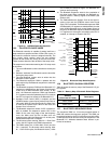
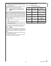
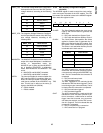
PREF_CFG The Positive Voltage Reference Configuration
field specifies the source of the ADC positive
voltage reference, according to the following
table:
NREF_CFG The Negative Voltage Reference Configura-
tion field specifies the source of the ADC neg-
ative voltage reference, according to the
following table:
MUXOUTEN
The MUXOUT Enable bit controls whether the
output of the Input Multiplexer is available ex-
ternally. In single-ended mode, the
MUXOUT0 pin is active and the MUXOUT1
pin is disabled (TRI-STATE). In differential
mode, both MUXOUT0 and MUXOUT1 are
active.
0 – MUXOUT0 and MUXOUT1 disabled.
1 – MUXOUT0 and MUXOUT1 enabled.
INTEN The Interrupt Enable bit controls whether the
ADC interrupt (IRQ13) is enabled. When en-
abled, the interrupt request is asserted when
valid data is available in the ADCRESLT reg-
ister. This bit has no effect on the wake_up
signal to the MIWU unit (WUI30).
0 – IRQ13 disabled.
1 – IRQ13 enabled.
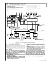
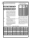
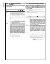
16.5.2 ADC Auxiliary Configuration Register
(ADCACR)
The ADCACR register is used to control the clock configu-
ration and report the status of the ADC module. The CPU
bus master has read/write access to the ADCACR register.
After reset, this register is clear.
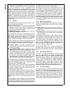
CLKSEL The Clock Select bit selects the clock source
used by the DELAY2 block to generate the
ADC clock.
0 – ADC clock derived from System Clock.
1 – ADC clock derived from Auxiliary Clock 2.
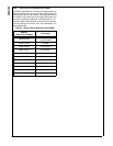
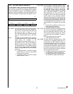
CLKDIV The Clock Divisor field specifies the divisor
applied to System Clock to generate the 12
MHz clock required by the ADC module. Only
the System Clock is affected by this divisor.
The divisor is not used when Auxiliary Clock 2
is selected as the clock source.
PRM The ADC Primed bit is a read-only bit that in-
dicates the ADC has been primed to perform
a conversion by writing to the ADCSTART reg-
ister. The bit is cleared after the conversion is
completed.
0 – ADC has not been primed.
1 – ADC has been primed.
TRG The ADC Triggered bit is a read-only bit that
indicates the ADC has been triggered. The bit
is set during any pre-conversion delay. The bit
is cleared after the conversion is completed.
0 – ADC has not been triggered.
1 – ADC has been triggered.
CNVT The ADC Conversion bit is a read-only bit that
indicates the ADC has been primed to per-
form a conversion, a valid internal or external
trigger event has occurred, any pre-conver-
sion delay has expired, and the ADC conver-
sion is in progress. The bit is cleared after the
conversion is completed.
0 – ADC is not performing a conversion.
1 – ADC conversion is in progress.
PREF_CFG PREF Source
00 Internal (AVCC)
01 VREFP
10 ADC0
11 ADC1
NREF_CFG NREF source
00 Internal (AGND)
01 Reserved
10 ADC2
11 ADC3
15 14 13 12 3 2 1 0
CNVT TRG PRM Reserved CLKDIV CLKSEL
CLKDIV Clock Divisor
00 1
01 2
10 4
11 Reserved


