53 www.national.com
CP3BT26
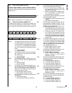
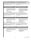
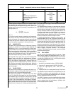
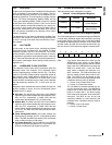
Choose capacitor component values in the tables to obtain
the specified load capacitance for the crystal when com-
bined with the parasitic capacitance of the trace, socket, and
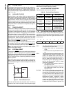
package (which can vary from 0 to 8 pF). As a guideline, the
load capacitance is:
C2 > C1
C1 can be trimmed to obtain the desired load capacitance.
The start-up time of the 32.768 kHz oscillator can vary from
one to six seconds. The long start-up time is due to the high
Q value and high serial resistance of the crystal necessary
to minimize power consumption in Power Save mode.
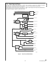
11.2 MAIN CLOCK
The Main Clock is generated by the 12-MHz high-frequency
oscillator or driven by an external signal (typically the
LMX5252 RF chip). It can be stopped by the Power Man-
agement Module to reduce power consumption during peri-
ods of reduced activity. When the Main Clock is restarted, a
14-bit timer generates a Good Main Clock signal after a
start-up delay of 32,768 clock cycles. This signal is an indi-
cator that the high-frequency oscillator is stable.
The Stop Main Osc signal from the Power Management
Module stops and starts the high-frequency oscillator.
When this signal is asserted, it presets the 14-bit timer to
3FFFh and stops the high-frequency oscillator. When the
signal goes inactive, the high-frequency oscillator starts and
the 14-bit timer counts down from its preset value. When the
timer reaches zero, it stops counting and asserts the Good
Main Clock signal.
11.3 SLOW CLOCK
The Slow Clock is necessary for operating the device in re-
duced power modes and to provide a clock source for mod-
ules such as the Timing and Watchdog Module.
The Slow Clock operates in a manner similar to the Main
Clock. The Stop Slow Osc signal from the Power Manage-
ment Module stops and starts the low-frequency (32.768
kHz) oscillator. When this signal is asserted, it presets a 6-
bit timer to 3Fh and disables the low-frequency oscillator.
When the signal goes inactive, the low-frequency oscillator
starts, and the 6-bit timer counts down from its preset value.
When the timer reaches zero, it stops counting and asserts
the Good Slow Clock signal, which indicates that the Slow
Clock is stable.
For systems that do not require a reduced power consump-
tion mode, the external crystal network may be omitted for
the Slow Clock. In that case, the Slow Clock can be synthe-
sized by dividing the Main Clock by a prescaler factor. The
prescaler circuit consists of a fixed divide-by-2 counter and
a programmable 8-bit prescaler register. This allows a
choice of clock divisors ranging from 2 to 512. The resulting
Slow Clock frequency must not exceed 100 kHz.
A software-programmable multiplexer selects either the
prescaled Main Clock or the 32.768 kHz oscillator as the
Slow Clock. At reset, the prescaled Main Clock is selected,
ensuring that the Slow Clock is always present initially. Se-
lection of the 32.768 kHz oscillator as the Slow Clock dis-
ables the clock prescaler, which allows the CLK1 oscillator
to be turned off, which reduces power consumption and ra-
diated emissions. This can be done only if the module de-
tects a toggling low-speed oscillator. If the low-speed
oscillator is not operating, the prescaler remains available
as the Slow Clock source.
11.4 PLL CLOCK
The PLL Clock is generated by the PLL from the 12 MHz
Main Clock by applying a multiplication factor of ×3, ×4, or
×5. The USB interface is clocked directly by the PLL Clock
and requires a 48 MHz clock, so a ×4 scaling factor must be
used if the USB interface is active.
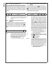
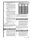
To enable the PLL:
1. Set the PLL multiplication factor in PRFSC.MODE.
2. Clear the PLL power-down bit CRCTRL.PLLPWD.
3. Clear the high-frequency clock select bit CRC-
TRL.FCLK.
4. Read CRCTRL.FCLK, and go back to step 3 if not clear.
The CRCTRL.FCLK bit will be clear only after the PLL has
stabilized, so software must repeat step 3 until the bit is
clear. The clock source can be switched back to the Main
Clock by setting the CRCTRL.FCLK bit.
The PRSFC register must not be modified while the System
Clock is derived from the PLL Clock. The System Clock
must be derived from the low-frequency oscillator clock
while the MODE field is modified.
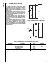
Table 22 Component Values of the Low Frequency Crystal Circuit
Component Parameters Values Tolerance
Crystal Resonance Frequency
Typ e
Maximum Serial Resistance
Maximum Shunt Capacitance
Load Capacitance
Min. Q factor
32.768 kHz
Parallel
N-Cut or XY-bar
40 kΩ
2 pF
12.5 pF
40000
N/A
Capacitor C1, C2 Capacitance 25 pF 20%
CL
C1 C2×
C1 C2+
---------------------
Cparasitic+=


