


FLL Operation from Low-Power Modes-
4-9FLL+ Clock Module
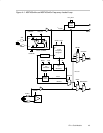
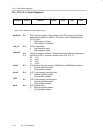
4.2.7 Disabling the FLL Hardware and Modulator
The FLL is disabled when the status register bit SCG0 = 1. When the FLL is
disabled, the DCO runs at the previously selected tap and DCOCLK is not
automatically stabilized.
The DCO modulator is disabled when SCFQ_M = 1. When the DCO modulator
is disabled, the DCOCLK is adjusted to the nearest of the available DCO taps.
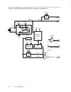
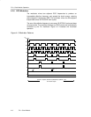
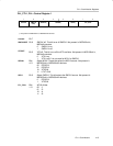
4.2.8 FLL Operation from Low-Power Modes-
An interrupt service request clears SCG1, CPUOFF and OSCOFF if set but
does not clear SCG0. This means that FLL operation from within an interrupt
service routine entered from LPM1, 2, 3 or 4, the FLL remains disabled and
the DCO operates at the previous setting as defined in SCFI0 and SCFI1.
SCG0 can be cleared by user software if FLL operation is required.
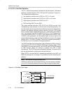
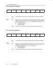
4.2.9 Buffered Clock Output
ACLK may be divided by 1, 2, 4, or 8 and buffered out of the device on P1.5.
The division rate is selected with the FLL_DIV bits.
The ACLK output is multiplexed with other pin functions. When multiplexed,
the pin must be configured for the ACLK output.
BIS.B #P1SEL_5,&P1SEL ; Select ACLK/n signal as
; output for port P1.5 if
BIS.B #P1DIR_5,&P1DIR ; Select port P1.5 to ACLK/n
; signal for output