Flash Memory Operation
5-14 Flash Memory Controller
5.3.4 Flash Memory Access During Write or Erase
When any write or any erase operation is initiated from RAM and while
BUSY=1, the CPU may not read or write to or from any flash location.
Otherwise, an access violation occurs, ACCVIFG is set, and the result is
unpredictable. Also if a write to flash is attempted with WRT=0, the ACCVIFG
interrupt flag is set, and the flash memory is unaffected.
When a byte/word write or any erase operation is initiated from within flash
memory, the flash controller returns op-code 03FFFh to the CPU at the next
instruction fetch. Op-code 03FFFh is the JMP PC instruction. This causes the
CPU to loop until the flash operation is finished. When the operation is finished
and BUSY=0, the flash controller allows the CPU to fetch the proper op-code
and program execution resumes.
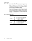
The flash access conditions while BUSY=1 are listed in Table 5−3.
Table 5−3.Flash Access While BUSY = 1
Flash
Operation
Flash
Access
WAIT Result
Read 0 ACCVIFG = 0. 03FFFh is the value read
Any erase, or
Write 0 ACCVIFG = 1. Write is ignored
Byte/word write
Instruction
fetch
0 ACCVIFG = 0. CPU fetches 03FFFh. This
is the JMP PC instruction.
Any 0 ACCVIFG = 1, LOCK = 1
Read 1 ACCVIFG = 0, 03FFFh is the value read
Block write
Write 1 ACCVIFG = 0, Write is ignored
Instruction
fetch
1 ACCVIFG = 1, LOCK = 1


