


Flash Memory Operation
5-4 Flash Memory Controller
5.3 Flash Memory Operation
The default mode of the flash memory is read mode. In read mode, the flash
memory is not being erased or written, the flash timing generator and voltage
generator are off, and the memory operates identically to ROM.
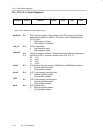
MSP430 flash memory is in-system programmable (ISP) without the need for
additional external voltage. The CPU can program its own flash memory. The
flash memory write/erase modes are selected with the BLKWRT, WRT,
MERAS, and ERASE bits and are:
- Byte/word write
- Block write
- Segment Erase
- Mass Erase (all main memory segments)
- All Erase (all segments)
Reading or writing to flash memory while it is being programmed or erased is
prohibited. If CPU execution is required during the write or erase, the code to
be executed must be in RAM. Any flash update can be initiated from within
flash memory or RAM.
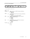
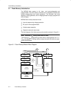
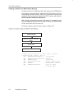
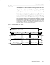
5.3.1 Flash Memory Timing Generator
Write and erase operations are controlled by the flash timing generator shown
in Figure 5−3. The flash timing generator operating frequency, f
FTG
, must be
in the range from ~ 257 kHz to ~ 476 kHz (see device-specific datasheet).
Figure 5−3. Flash Memory Timing Generator Block Diagram
FN5 FN0
PUC
...........
EMEX
Flash Timing Generator
Divider, 1−64
BUSY WAIT
Reset
f
(FTG)
FSSELx
SMCLK
SMCLK
ACLK
MCLK
00
01
10
11
The flash timing generator can be sourced from ACLK, SMCLK, or MCLK. The
selected clock source should be divided using the FNx bits to meet the
frequency requirements for f
FTG
. If the f
FTG
frequency deviates from the
specification during the write or erase operation, the result of the write or erase
may be unpredictable, or the flash memory may be stressed above the limits
of reliable operation.