


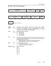
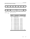

SD16 Operation
21-4 SD16
21.2 SD16 Operation
The SD16 module is configured with user software. The setup and operation
of the SD16 is discussed in the following sections.
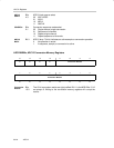
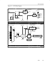
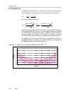
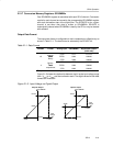
21.2.1 ADC Core
The analog-to-digital conversion is performed by a 1-bit, second-order
sigma-delta modulator. A single-bit comparator within the modulator quantizes
the input signal with the modulator frequency f
M
. The resulting 1-bit data
stream is averaged by the digital filter for the conversion result.
21.2.2 Analog Input Range and PGA
The full-scale input voltage range for each analog input pair is dependent on
the gain setting of the programmable gain amplifier of each channel. The
maximum full-scale range is ±V
FSR
where V
FSR
is defined by:
V
FSR
+
V
REF
ń
2
GAIN
PGA
For a 1.2V reference, the maximum full-scale input range for a gain of 1 is:
" V
FSR
+
1.2V
ń
2
1
+" 0.6V
Refer to the device-specific data sheet for full-scale input specifications.
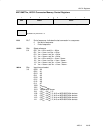
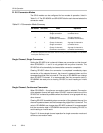
21.2.3 Voltage Reference Generator
The SD16 module has a built-in 1.2V reference that can be used for each SD16
channel and is enabled by the SD16REFON bit. When using the internal
reference an external 100nF capacitor connected from V
REF
to AV
SS
is
recommended to reduce noise. The internal reference voltage can be used
off-chip when SD16VMIDON = 1. The buffered output can provide up to 1mA
of drive. When using the internal reference off-chip, a 470nF capacitor
connected from V
REF
to AV
SS
is required. See device-specific data sheet for
parameters.
An external voltage reference can be applied to the V
REF
input when
SD16REFON and SD16VMIDON are both reset.
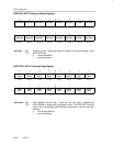
21.2.4 Auto Power-Down
The SD16 is designed for low power applications. When the SD16 is not
actively converting, it is automatically disabled and automatically re-enabled
when needed. The reference is not automatically disabled, but can be disabled
by setting SD16REFON = 0. When the SD16 or reference are disabled, they
consume no current.