DAC12 Operation
23-5DAC12
23.2 DAC12 Operation
The DAC12 module is configured with user software. The setup and operation
of the DAC12 is discussed in the following sections.
23.2.1 DAC12 Core
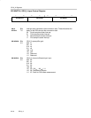
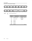
The DAC12 can be configured to operate in 8- or 12-bit mode using the
DAC12RES bit. The full-scale output is programmable to be 1x or 3x the
selected reference voltage via the DAC12IR bit. This feature allows the user
to control the dynamic range of the DAC12. The DAC12DF bit allows the user
to select between straight binary data and 2’s compliment data for the DAC.
When using straight binary data format, the formula for the output voltage is
given in Table 23−1.
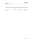
Table 23−1.DAC12 Full-Scale Range (Vref = V
eREF+
or V
REF+
)
Resolution DAC12RES DAC12IR Output Voltage Formula
12 bit 0 0
Vout + Vref 3
DAC12_xDAT
4096
12 bit 0 1
Vout + Vref
DAC12_xDAT
4096
8 bit 1 0
Vout + Vref 3
DAC12_xDAT
256
8 bit 1 1
Vout + Vref
DAC12_xDAT
256
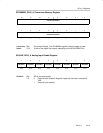
In 8-bit mode the maximum useable value for DAC12_xDAT is 0FFh and in
12-bit mode the maximum useable value for DAC12_xDAT is 0FFFh. Values
greater than these may be written to the register, but all leading bits are
ignored.
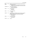
DAC12 Port Selection
On MSP430FG43x devices, the DAC12 outputs are multiplexed with the port
P6 pins and ADC12 analog inputs, and also the VeREF+ and P5.1/S0/A12
pins. When DAC12AMPx > 0, the DAC12 function is automatically selected for
the pin, regardless of the state of the associated PxSELx and PxDIRx bits. The
DAC12OPS bit selects between the P6 pins and the VeREF+ and P5.1 pins
for the DAC outputs. For example, when DAC12OPS = 0, DAC12_0 outputs
on P6.6 and DAC12_1 outputs on P6.7. When DAC12OPS = 1, DAC12_0
outputs on VeREF+ and DAC12_1 outputs on P5.1. See the port pin schematic
in the device-specific datasheet for more details.
On MSP430x42x0 devices, the DAC12 output is multiplexed with the port
P1.4/A3− pin. In this case, the DAC12OPS bit selects the DAC function for the
pin. See the port pin schematic in the device-specific datasheet for more
details.


