


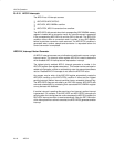
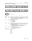
ADC12 Registers
20-23ADC12
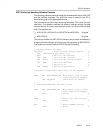
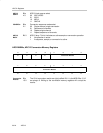
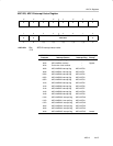
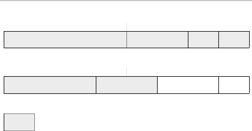
ADC12CTL1, ADC12 Control Register 1
15 14 13 12 11 10 9 8
CSTARTADDx SHSx SHP ISSH
rw−(0) rw−(0) rw−(0) rw−(0) rw−(0) rw−(0) rw−(0) rw−(0)
76543210
ADC12DIVx ADC12SSELx CONSEQx
ADC12
BUSY
rw−(0) rw−(0) rw−(0) rw−(0) rw−(0) rw−(0) rw−(0) r−(0)
Modifiable only when ENC = 0
CSTART
ADDx
Bits
15-12
Conversion start address. These bits select which ADC12
conversion-memory register is used for a single conversion or for the first
conversion in a sequence. The value of CSTARTADDx is 0 to 0Fh,
corresponding to ADC12MEM0 to ADC12MEM15.
SHSx
Bits
11-10
Sample-and-hold source select
00 ADC12SC bit
01 Timer_A.OUT1
10 Timer_B.OUT0
11 Timer_B.OUT1
SHP
Bit 9 Sample-and-hold pulse-mode select. This bit selects the source of the
sampling signal (SAMPCON) to be either the output of the sampling timer or
the sample-input signal directly.
0 SAMPCON signal is sourced from the sample-input signal.
1 SAMPCON signal is sourced from the sampling timer.
ISSH
Bit 8 Invert signal sample-and-hold
0 The sample-input signal is not inverted.
1 The sample-input signal is inverted.
ADC12DIVx
Bits
7-5
ADC12 clock divider
000 /1
001 /2
010 /3
011 /4
100 /5
101 /6
110 /7
111 /8