


SD16 Operation
21-9SD16
21.2.7 Conversion Memory Registers: SD16MEMx
One SD16MEMx register is associated with each SD16 channel. Conversion
results for each channel are moved to the corresponding SD16MEMx register
with each decimation step of the digital filter. The SD16IFG bit for a given
channel is set when new data is written to SD16MEMx. SD16IFG is
automatically cleared when SD16MEMx is read by the CPU or may be cleared
with software.
Output Data Format
The output data format is configurable in two’s complement or offset binary as
shown in Table 21−1.The data format is selected by the SD16DF bit.
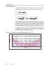
Table 21−1.Data Format
SD16DF Format Analog Input SD16MEMx
†
Digital Filter Output
(OSR =256)
+FSR FFFF FFFFFF
0
Unipolar:
Offset
ZERO 8000 800000
0
Offset
Binary
−FSR 0000 000000
+FSR
7FFF 7FFFFF
1
Bipolar:
Two’s
ZERO 0000 000000
1
Two’s
complement
−FSR 8000 800000
†
Independent of SD16OSRx setting; SD16LSBACC = 0.
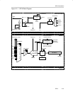
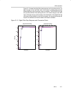
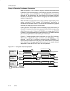
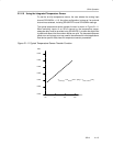
Figure 21−5 shows the relationship between the full-scale input voltage range
from −V
FSR
to +V
FSR
and the conversion result. The digital values for both data
formats are illustrated.
Figure 21−5. Input Voltage vs. Digital Output
Input
Voltage
SD16MEMx
−V
FSR
+V
FSR
7FFFh
8000h
Bipolar Output
Input
Voltage
SD16MEMx
−V
FSR
+V
FSR
FFFFh
8000h
Unipolar Output
0000h
0000h