Digital I/O Operation
9-5Digital I/O
9.2.5 P1 and P2 Interrupts
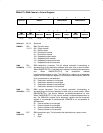
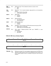
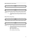
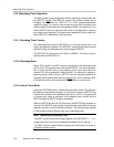
Each pin in ports P1 and P2 have interrupt capability, configured with the
PxIFG, PxIE, and PxIES registers. All P1 pins source a single interrupt vector,
and all P2 pins source a different single interrupt vector. The PxIFG register
can be tested to determine the source of a P1 or P2 interrupt.
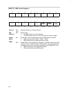
Interrupt Flag Registers P1IFG, P2IFG
Each PxIFGx bit is the interrupt flag for its corresponding I/O pin and is set
when the selected input signal edge occurs at the pin. All PxIFGx interrupt
flags request an interrupt when their corresponding PxIE bit and the GIE bit
are set. Each PxIFG flag must be reset with software. Software can also set
each PxIFG flag, providing a way to generate a software initiated interrupt.
Bit = 0: No interrupt is pending
Bit = 1: An interrupt is pending
Only transitions, not static levels, cause interrupts. If any PxIFGx flag becomes
set during a Px interrupt service routine, or is set after the RETI instruction of
a Px interrupt service routine is executed, the set PxIFGx flag generates
another interrupt. This ensures that each transition is acknowledged.
Note: PxIFG Flags When Changing PxOUT or PxDIR
Writing to P1OUT, P1DIR, P2OUT, or P2DIR can result in setting the
corresponding P1IFG or P2IFG flags.
Note: Length of I/O Pin Interrupt Event
Any external interrupt event should be at least 1.5 times MCLK or longer, to
ensure that it is accepted and the corresponding interrupt flag is set.


