


ADC12 Introduction
20-2 ADC12
20.1 ADC12 Introduction
The ADC12 module supports fast, 12-bit analog-to-digital conversions. The
module implements a 12-bit SAR core, sample select control, reference
generator and a 16 word conversion-and-control buffer. The
conversion-and-control buffer allows up to 16 independent ADC samples to be
converted and stored without any CPU intervention.
ADC12 features include:
- Greater than 200 ksps maximum conversion rate
- Monotonic 12-bit converter with no missing codes
- Sample-and-hold with programmable sampling periods controlled by
software or timers.
- Conversion initiation by software, Timer_A, or Timer_B
- Software selectable on-chip reference voltage generation (1.5 V or 2.5 V)
- Software selectable internal or external reference
- Eight individually configurable external input channels (twelve on
MSP430FG43x devices)
- Conversion channels for internal temperature sensor, AV
CC
, and external
references
- Independent channel-selectable reference sources for both positive and
negative references
- Selectable conversion clock source
- Single-channel, repeat-single-channel, sequence, and repeat-sequence
conversion modes
- ADC core and reference voltage can be powered down separately
- Interrupt vector register for fast decoding of 18 ADC interrupts
- 16 conversion-result storage registers
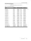
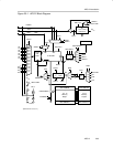
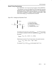
The block diagram of ADC12 is shown in Figure 20−1.