


ADC12 Operation
20-4 ADC12
20.2 ADC12 Operation
The ADC12 module is configured with user software. The setup and operation
of the ADC12 is discussed in the following sections.
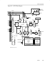
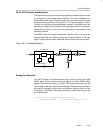
20.2.1 12-Bit ADC Core
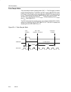
The ADC core converts an analog input to its 12-bit digital representation and
stores the result in conversion memory. The core uses two
programmable/selectable voltage levels (V
R+
and V
R−
) to define the upper and
lower limits of the conversion. The digital output (N
ADC
) is full scale (0FFFh)
when the input signal is equal to or higher than V
R+
, and zero when the input
signal is equal to or lower than V
R−
. The input channel and the reference
voltage levels (V
R+
and V
R−
) are defined in the conversion-control memory.
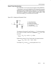
The conversion formula for the ADC result N
ADC
is:
N
ADC
+ 4095
Vin * V
R*
V
R)
* V
R*
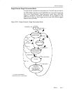
The ADC12 core is configured by two control registers, ADC12CTL0 and
ADC12CTL1. The core is enabled with the ADC12ON bit. The ADC12 can be
turned off when not in use to save power. With few exceptions the ADC12
control bits can only be modified when ENC = 0. ENC must be set to 1 before
any conversion can take place.
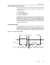
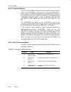
Conversion Clock Selection
The ADC12CLK is used both as the conversion clock and to generate the
sampling period when the pulse sampling mode is selected. The ADC12
source clock is selected using the ADC12SSELx bits and can be divided from
1-8 using the ADC12DIVx bits. Possible ADC12CLK sources are SMCLK,
MCLK, ACLK, and an internal oscillator ADC12OSC.
The ADC12OSC, generated internally, is in the 5-MHz range, but varies with
individual devices, supply voltage, and temperature. See the device-specific
datasheet for the ADC12OSC specification.
The user must ensure that the clock chosen for ADC12CLK remains active
until the end of a conversion. If the clock is removed during a conversion, the
operation will not complete and any result will be invalid.