Theory of Operation
1780R-Series Service Manual
3–71
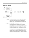
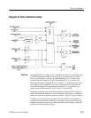
The input H sync pulse width, which is regenerated, is approximately a half line
in duration. In order to provide a uniform duration, usable H sync is shaped by a
monostable pulse shaper. Its output is supplied to the Differential Gain and Phase
circuits as well as to the Blanking Logic.
The Center Dot Blanking Logic, which consists of NOR and NAND gates,
outputs the Vectorscope blanking pulse and the horizontal sync used by the Pix
Mon H-Sweep Generator.
SCH/Chroma Switching. U452 is used as a chroma switch. The Vectorscope
chroma signal is input to one emitter, while the SCH signal is input to the other.
The chroma signal, through pin 3, originates from the Vectorscope Chroma Gain
Cell on Diagram 25. There is a peaking circuit that consists of C554, R550, and
R554 which sets the gain in this input.
The SCH signal from the Sync Locked OSC (Diagram 15) is differential. The
combination of Q663 and Q665 is a differential receiver that outputs a single-en-
ded sine-wave signal to a low-pass filter. The amplitude of the sine wave is
controlled by the SCH Gain (R667) adjustment. The low-pass filter is made up
of C661, L659, and C660. The filtered sine-wave output signal is AC-coupled to
pin 2 of U452.
Switching is controlled by the VEC line from U653, pin 12. When VEC is low,
Vectorscope chroma signal current flows out U452 pin 12 into the emitter
follower stage (Q447); SCH signal current is switched into the power supply
from pin 6. When VEC is high the opposite condition occurs and SCH signal
current flows into the emitter follower stage.
Control Signal Generator. Signals to control timing and blanking of the Vector-
scope display are generated in a Programmed Logic Array (PLA), U653. It
combines the levels of static control lines /SCH and /VECTOR EN, with the
dynamic control line states of /FLD SCH BLK and FLD CHROMA SW, along
with a counter output correctly timed to these control signals.
U757 is used as a buffer for the chroma signal from the Demodulator (Diagram
28). Its Subcarrier output is a direct input to U653. The /Subcarrier output is the
A input to U751A, which is the lower order half of an 8-bit ripple through the
counter; U751B is the higher order half of the counter. All eight outputs from the
counter are input to U653 providing the PLA with up to 256 possible decisions
for one complete cycle of the counter. The line rate timing signal for U653 is the
INPUT H SYNC from the H & V Sync Generators (Diagram 9). INPUT H
SYNC from Diagram 9 goes through the MPU Interconnects on Diagrams 12,
44, and 25 to Diagram 27.
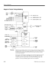
Center Dot Comparator. The Vertical and Horizontal Deflection Amplifier input
signals drive the + and – comparators (U424). If the CRT-displayed signal is
Circuit Theory


