Theory of Operation
3–8
1780R-Series Service Manual
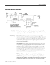
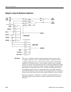
The voltage follower drives a current-mode feedback amplifier consisting of
Q492, Q390, and Q294. The gain is set by the feedback network consisting of
R393, R396, R394, R295, and Q295. When the instrument is configured for X1
probe gain, Q295 is off and R393 and R396 set the amplifier gain to 1.1. In the
X10 gain setting, Q295 is saturated and the feedback signal from R393 is
shunted to ground through R394 and R295. This causes the gain of the amplifier
to increase to X11 when R295 is properly adjusted. Gain switching allows the
1780R-Series to work with either X1 or X10 probes.
The operating point of the Probe Input Amplifier is established by a feedback
loop consisting of U490, R491, C490, and R492. The loop tries to keep the
emitter of Q492 at 0 V. U490, R491, and C490 form a inverting integrator which
compares the voltage on Q492’s emitter to 0 V. If the emitter is not at 0 V, then
the charge on C490 will change, and the voltage on U490 pin 6 will move in a
direction opposite to the error at Q492’s emitter. This voltage is applied to the
amplifier input through R492, forcing Q492’s emitter back to 0 V. The feedback
loop compensates for offset variations in Q493 and Q492 and prevents output
DC level shifts when the gain is changed from X1 to X10.
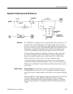
Probe Calibrator. The Calibrator provides a 1 volt square wave at the front-panel
CAL OUT pin jack. The Cal Timing signal, that originates from the Calibrator
and Filter Control (Diagram 7), alternately saturates and turns off Q897. The
Calibrator Amplitude (R795) sets the cathode potential on VR796 (collector
voltage for Q897) to 5 volts. When Q897 is turned off, a voltage divider (R897,
R898, and R899) sets the Probe Cal Out to 1 volt. When Q897 is saturated, the
Probe Cal Out is at ground.
Probe Output Amp. The Probe Output Amplifier consists of a variable attenuator
and a X2 gain non-inverting amplifier, together providing a gain of 0.9. When
combined with the X1.1/X11.1 gain of the Probe Input Amplifier, an overall
probe system gain of X1/X10 results.
R1106, R1107, and R1108 form the attenuator. R1107 adjusts the overall probe
system gain. Q1111, Q1218, Q1113, and Q1115 form the amplifier. Feedback
resistors R1116 and R1218 set the gain of 2. C1222 varies the amplifier
frequency response and is used to adjust the overall probe system response.
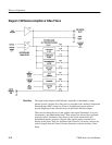
DC Restorer. Either the backporch or sync tip level of the applied video can be
clamped to 0 volts by the DC Restorer circuit, which consists of U1217 and
U1211. U1217 is a gated transconductance amplifier that samples the filtered
output of the Probe Amplifier during either sync tip or backporch (depending on
the timing of the sample pulse at pin 5). R1122, C1221, L1220, and C1220 (at
the inverting input, pin 2 input of U1217) form a low-pass filter, with a notch at
the subcarrier frequency. U1217 drives C1216, which holds charge during the
active portion of the video line. When Q1309 is on, C1313 is in parallel with
C1216, and the DC Restorer response is slowed so that 60 Hz (50 Hz for 1781)


