Theory of Operation
1780R-Series Service Manual
3–93
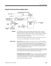
Storage. The data stored in Static Random Access Memory (U251 and U260) is
from the conversion of the previously-sampled video line and is at the same
point that the A/D Converter is outputting from the current line. During the read
operation, the 12-bit Memory data is on the M Data Bus and is being input to the
Adder (U440, U441, and U450). The lower 8 bits, on the M Data Bus, are
inverted and input to the Subtracter (U461A, B, C, D and U470B, C, E, F).
During a write operation, data from either the Bypass Buffer or the Filter Latch
is stored in Memory. U330 is a quad, dual-input multiplexer used as a memory
switch, whose output is controlled by the level of the Memory Access pulse
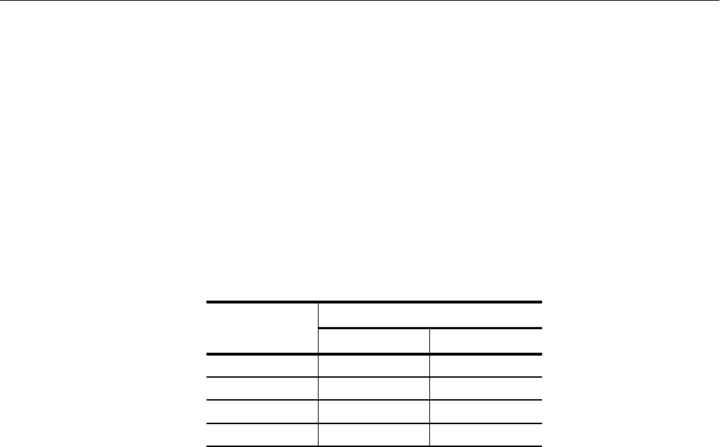
(/MA). See Table 3–4.
Table 3–4: Memory Switch Outputs
U33 p
/MA
U33
0 Out
p
ut
High Low
/OE (PIN 4) /CLOCK2 /RD
/WE (PIN 7) R/W /WR
/CSL (PIN 9) Ground A8
/CSH (PIN 12) Ground /A8
The R/W pulse is derived from the rising edge of inverted Clock2 (U470D) and
clocks U400A (high for a write operation) and outputs the /W from the inverted
output of U400A (pin 6). Clock (8 MHz) switches the inverted output of U400A
to a high state after a quarter of a Clock2 cycle, and enables the Memory to store
data before the next address change.
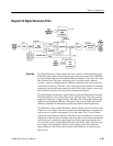
Address Counter and CPU Access. The Address Counter (U271) is a multi-mode,
9-bit synchronous counter, built from a Programmable Logic Array. During
filtering, it operates as an 8-bit counter phase-locked by the 2 ms AFC sync
pulse, from the AFC Counter. The ninth bit is used to pass the /DG Filter pulse
during DP/DG display modes. Output A6, inverted by U461F, is the clock for
the Memory Write Control. When /MA is low, /BYPASS is used to clear the
counter and the INC input is used to increment the counter for Memory access
by the Microprocessor.
CPU Access, made up of a 16-input Programmable Logic Array (U261) and a
D-type flip-flop (U400B), provides addressing for the upper pages of Storage
and generates the INC pulse for the Address Counter. When /PAL is low, the +V
Out becomes address bit A9. AB1 is latched with the /WR signal when /Fltr Brd
is low to become address bit A10. When /PAL is high, AB0 is latched and used
for address bit A9.
The CPU Access (U261 and U400B) also operates as a one-bit state machine that
increments the Memory addresses during data transfer to the Microprocessor.


