Theory of Operation
3–92
1780R-Series Service Manual
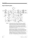
The D/A Converter latches data off the M Data Bus at the same time that the
Adder data is loaded into the Filter Latch. The analog signal is output to a
low-pass output filter to remove sampling artifacts above approximately
750 kHz.
The Address Counter output A6 is the clock for the Memory Write Control. The
CPU Access provides addressing for the upper pages of Memory. It also controls
the one-bit state machine that increments the memory addresses during data
transfer to the Microprocessor.
The Microprocessor accesses the Recursive Filter Storage through the CPU Bus
Interface. For full field operation, a state machine is used as a half-line counter to
inhibit Write Enable during the vertical interval and prevent writing to Memory.
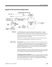
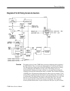
A/D Converter. The demodulated chrominance signal (Demod) from the Differen-
tial Phase and Gain Demodulator (Diagram 26) is the analog input to the A/D
Converter section of U210. R210 is a protection resistor. The analog input is
sampled on the falling edge of a 4 MHz clock (/Clock2), and data is output on
the C Data Bus at the falling edge of the next clock pulse. The C Data Bus is the
8-bit input to the Subtracter (U240 and U430) and the Bypass Buffer (U230 and
U270).
Subtracter. The upper 8 bits of data, from Storage, that are on the M Data Bus are
inverted (U461 and U470) and added to the input data (a logical subtraction).
Adder. The Subtracter output (S Data Bus) is input, as an error signal, to the
Adder lower 8 bits (U450 and U441). The Subtracter borrow output (C4) is
inverted (U470A) and input as an error signal for the upper 4 bits of the 12-bit
Adder (U440 plus U441 and U450). The U450 Carry (C4) increments U440 and
adds a hexadecimal F to decrement. The 12 bits of Adder output data are latched
into memory, from the P Data Bus, on the falling edge of /Clock2 by U250 and
U451 (octal, tri-state, flip-flops) that are the Filter Latch.
Data Switch. U410B is the Data Switch that controls the source of data to the M
Data Bus during filtering. It activates the tri-state output of either the Filter Latch
(U250 and U451) or the Bypass Buffer (U230 and U270) as selected by the R/W
pulse. When /BYPASS and /MA are both high, data is output from the Filter
Latch to Storage. When /BYPASS is low and /MA is high, data output is from
the Bypass Buffer.
D/A Converter. The D/A Converter, contained in U210, latches data off the M
Data Bus on the falling edge of Clock2, at the same time as the Adder output
data is loaded into the Filter Latch. On the rising edge of Clock2, the analog
signal is output to a 4-pole Sallen and Keyes low-pass output filter (Q310 and
Q320) which removes sampling artifacts above approximately 750 kHz.
Circuit Theory


