


User’s Manual
IBM PowerPC 750GX and 750GL RISC Microprocessor
Instruction-Cache and Data-Cache Operation
Page 122 of 377
gx_03.fm.(1.2)
March 27, 2006
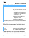
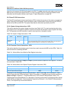
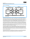
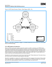
Both caches are tightly coupled into the 750GX’s bus interface unit (BIU) to allow efficient access to the
system memory controller and other bus masters. The bus interface unit receives requests for bus operations
from the instruction and data caches, and executes the operations per the 60x bus protocol. The BIU
provides address queues, prioritizing logic, and bus control logic. The BIU captures snoop addresses for data
cache, address queue, and memory reservation (lwarx and stwcx. instruction) operations. In the 750GX, an
L1 cache miss first accesses the L2 cache to find the desired cache block before accessing the BIU.
The data cache provides buffers for load-and-store bus operations. All the data for the corresponding address
queues (load-and-store data queues) is located in the data cache. The data queues are considered tempo-
rary storage for the cache and not part of the BIU. The data cache also provides storage for the cache tags
required for memory coherency and performs the cache-block-replacement PLRU function. The data cache is
supported by two cache-block reload/write-back buffers. This allows a cache block to be loaded or unloaded
from the cache in a single cycle. See Figure 9-1 on page 327.
The data cache supplies data to the General Purpose Registers (GPRs) and Floating Point Registers (FPRs)
by means of the load/store unit (LSU). The 750GX’s LSU is directly coupled to the data cache to allow effi-
cient movement of data to and from the GPRs and FPRs. The LSU provides all logic required to calculate
effective addresses, handles data alignment to and from the data cache, and provides sequencing for load-
and-store string and multiple operations. Write operations to the data cache can be performed on a byte, half-
word, word, or double-word basis.
The instruction cache provides a 128-bit interface to the instruction unit, so four instructions can be made
available to the instruction unit in a single clock cycle. The instruction unit accesses the instruction cache
frequently in order to sustain the high throughput provided by the 6-entry instruction queue.
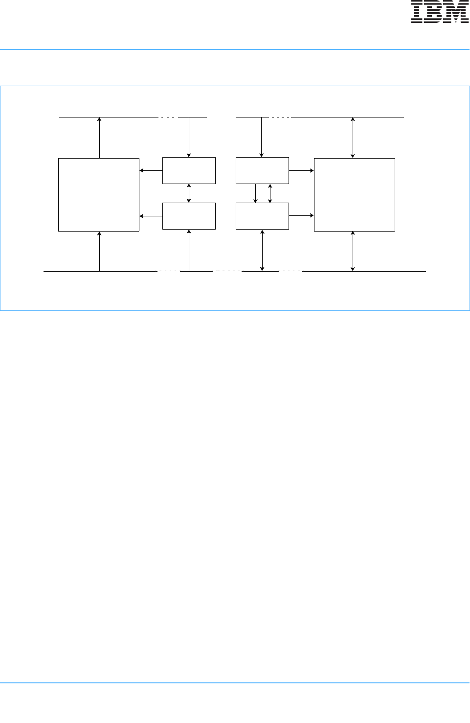
Figure 3-1. Cache Integration
Instruction Unit
Load/Store Unit
Cache Tags
(LSU)
Instructions (0–127)
Instructions (0–63)
Instruction Cache
32-KB
8-Way Set Associative
Cache Logic
EA (20–26)
PA (0–19)
PA (0–31)
Cache Tags
Cache Logic
Data Cache
32-KB
8-Way Set Associative
Data (0–63)
Data (0–63)
EA: Effective Address
PA: Physical Address
MMU/L2/60x BIU