


User’s Manual
IBM PowerPC 750GX and 750GL RISC Microprocessor
Power and Thermal Management
Page 342 of 377
gx_10.fm.(1.2)
March 27, 2006
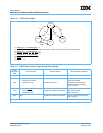
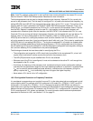
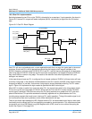
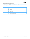
10.3.3 Dual PLL Implementation
Switching between the two PLLs on the 750GX is intended to be a seamless, 3-cycle operation. As shown in
Figure 10-2, the two PLL outputs will feed a multiplexer (MUX), controlled by a signal from the PLL select
logic.
Each PLL will use as a feedback path, a clock regeneration path that is a copy of a typical path in the actual
clock tree. Since both PLLs will be generating outputs that are integral or half integral multiples of the
SYSCLK frequency, all three clocks (SYSCLK, PLL0, and PLL1 out) will have a rising edge on (at least) every
other rising edge of SYSCLK. When the two PLLs are both configured for half integral multiples of SYSCLK,
they cannot have a common rising edge. This leads to the restriction that switching between half cycle
settings is not allowed.
In the case where at least one PLL is configured for an integral multiple of SYSCLK, all three clocks will have
a common rising edge. In the absence of skew between the two PLL outputs, the MUX control signal could be
changed just before, or just after, that common rising edge to achieve seamless switching. The PLL select
logic in Figure 10-2 represents the logic needed to generate the MUX control signal.
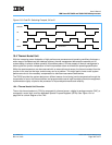
When HID1 is written to switch from one to the other PLL, the control logic waits for the rising edges of both
PLLs to line up with the rising edge of SYSCLK. When both the PLL0 and PLL1 clocks are high, the MUX
control signal is switched. If the bus/core ratio of the PLL being switched to is greater than 2.5x, one clock
pulse will be blocked. This provides seamless functionality regardless of any skew between the PLLs,
including snoop requests that could come in during a PLL switch operation. Timing of the switch signal is crit-
ical to ensure that there are no glitches or short clocks distributed to the logic.
There is also fence logic between the HID1 Register and the PLL and associated control logic to allow reset
functionality and to prevent the PLLs from becoming corrupted by a scan operation. This requirement allows
an operation such as a RISCWatch Long Shift Register Latch (LSRL) scan to occur without corrupting the
clocks. See Figure 10-3 on page 343.
Figure 10-2. Dual PLL Block Diagram
M
U
X
HID1 [PC0]
HID1 [PR0]
PLL_CFG ||
PLL_RNG
PLL0
PLL0 Feedback
M
U
X
P clk
Cloc
k
Tree
PLL
Select
Logic
HID1 [PS]
PLL1 Feedback
SYS CLK
HID1 [PC1] ||
HID1 [PR1]
PLL1
HID1 [PI0]
HID1