


User’s Manual
IBM PowerPC 750GX and 750GL RISC Microprocessor
Bus Interface Operation
Page 292 of 377
gx_08.fm.(1.2)
March 27, 2006
System designers should note that it is possible to ignore the ABB signal, and regenerate the state of ABB
locally within each device by monitoring the TS
and AACK input signals. The 750GX allows this operation by
using both the ABB
input signal and a locally regenerated version of ABB to determine if a qualified bus grant
state exists (both sources are internally ORed together). The ABB
signal can only be ignored if ABB and TS
are asserted simultaneously by all masters, or where arbitration (through assertion of BG
) is properly
managed in cases where the regenerated ABB
might not properly track the ABB signal on the bus. If the
750GX’s ABB
signal is ignored by the system, it must be connected to a pull-up resistor to ensure proper
operation. Additionally, the 750GX will not qualify a bus grant during the cycle that TS
is asserted on the bus
by any master. Address-bus arbitration without the use of the ABB
signal requires that every assertion of TS
be acknowledged by an assertion of AACK
while the processor is not in sleep mode.
8.3.2 Address Transfer
During the address transfer, the physical address and all attributes of the transaction are transferred from the
bus master to the slave devices. Snooping logic can monitor the transfer to enforce cache coherency; see the
discussion of snooping in Section 8.3.3, Address Transfer Termination, on page 300.
The signals used in the address transfer include the following signal groups:
• Address transfer start signal: transfer start (TS
)
• Address transfer signals: address bus (A[0–31]), and address parity (AP[0–3])
• Address transfer attribute signals: transfer type (TT[0–4]), transfer size (TSIZ[0–2]), transfer burst
(TBST
), cache inhibit (CI), write-through (WT), and global (GBL)
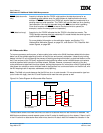
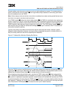
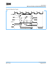
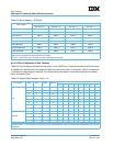
Figure 8-8 on page 293 shows that the timing for all of these signals, except TS
, is identical. All of the
address transfer and address transfer attribute signals are combined into the ADDR+ grouping in Figure 8-8.
The TS
signal indicates that the 750GX has begun an address transfer and that the address and transfer
attributes are valid (within the context of a synchronous bus). The 750GX always asserts TS
coincident with
ABB
. As an input, TS need not coincide with the assertion of ABB on the bus (that is, TS can be asserted
with, or on, a subsequent clock cycle after ABB
is asserted; the 750GX tracks this transaction correctly).
In Figure 8-8, the address transfer occurs during bus clock cycles 1 and 2 (arbitration occurs in bus clock
cycle 0 and the address transfer is terminated in bus clock 3). In this diagram, the address-bus termination
input, AACK, is asserted to the 750GX on the bus clock following assertion of TS (as shown by the depen-
dency line). This is the minimum duration of the address transfer for the 750GX; the duration can be extended
by delaying the assertion of AACK
for one or more bus clocks.