


User’s Manual
IBM PowerPC 750GX and 750GL RISC Microprocessor
gx_11.fm.(1.2)
March 27, 2006
Performance Monitor and System Related Features
Page 357 of 377
11.6 Debug Support
11.6.1 Overview
The 750GX provides the following debug support features:
• Branch trace
• Single step instruction trace
• Instruction-address breakpoint
• Data-address breakpoint
• Externally triggered soft stop
The trace mode allows either a single step trace if MSR[SE] = 1 or a branch trace if MSR[BE] = 1. The
instruction-address breakpoint and data-address breakpoint modes are invoked by setting the appropriate
bits in the Instruction Address Breakpoint Register (IABR) and Data Address Breakpoint Register (DABR).
Each of these debug features except for data-address breakpoint is a common feature of PowerPC devices.
The variances are noted in the following paragraphs.
11.6.2 Data-Address Breakpoint
The data-address breakpoint feature is controlled by the DABR Special Purpose Register which is described
in Section 4.5.17, Data Address Breakpoint Exception, on page 175. The data-address breakpoint action can
be one of the following:
• Data-storage interrupt (DSI)
•Soft stop
• Hard stop
A DSI on a data access does not complete the interrupting instruction.
11.7 JTAG/COP Functions
11.7.1 Introduction
The 750GX implements the Joint Test Action Group (JTAG) and common on-chip processor (COP) functions
for facilitating board testing and chip debug. The JTAG boundary scan features are used for board testing,
while the COP features are used mainly for system debug using a RISCWatch. The JTAG features and the
interface are fully compliant with the IEEE 1149.1a-1993 standard. The COP functions are compliant with the
JTAG standard whenever possible, and the COP external interface adheres to the IEEE 1149.1a-1993 serial
protocol. In this document, IEEE 1149.1a-1993 and JTAG are used interchangeably. The 750GX does
support the optional test reset pin.
11.7.2 Processor Resources Available through JTAG/COP Serial Interface
The shift register latches (SRLs) on the 750GX are linked so that data can be shifted serially through them to
either control or observe resources (such as caches and register files) within the processor. Various chain
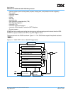
configurations are selected by the COP and placed between the JTAG TDI and TDO pins as shown in Figure
11-1, 750GX IEEE 1149.1a-1993/COP Organization, on page 358. RISCWatch configures and controls the
appropriate SRL chains to read and write various processor resources for system debug, including: