


User’s Manual
IBM PowerPC 750GX and 750GL RISC Microprocessor
gx_02.fm.(1.2)
March 27, 2006
Programming Model
Page 67 of 377
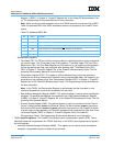
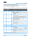
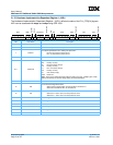
18 ILOCK
Instruction-cache lock
0 Normal operation.
1 Instruction cache is locked. A locked cache supplies data normally on a hit, but is
treated as a cache-inhibited transaction on a miss. On a miss, the transaction to
the bus or the L2 cache is single-beat. However, CI
still reflects the original state
as determined by address translation independent of cache locked or disabled
status.
To prevent locking during a cache access, an Instruction Synchronization (isync) instruc-
tion must precede the setting of ILOCK.
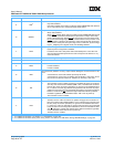
19 DLOCK
Data-cache lock.
0 Normal operation.
1 Data cache is locked. A locked cache supplies data normally on a hit, but is
treated as a cache-inhibited transaction on a miss. On a miss, the transaction to
the bus or the L2 cache is single-beat. However, CI
still reflects the original state
as determined by address translation independent of cache locked or disabled
status. A snoop hit to a locked L1 data cache performs as if the cache were not
locked. A cache block invalidated by a snoop remains invalid until the cache is
unlocked.
To prevent locking during a cache access, a sync instruction must precede the setting of
DLOCK.
20 ICFI
Instruction-cache flash invalidate
0 The instruction cache is not invalidated. The bit is cleared when the invalidation
operation begins (usually the next cycle after the write operation to the register).
The instruction cache must be enabled for the invalidation to occur.
1 An invalidate operation is issued that marks the state of each instruction-cache
block as invalid without writing back modified cache blocks to memory. Cache
access is blocked during this time. Bus accesses to the cache are signaled as
misses during invalidate-all operations. Setting ICFI clears all the valid bits of the
blocks and the pseudo least-recently used (PLRU) bits to point to way L0 of each
set. Once the L1 flash invalidate bits are set through an mtspr operation, hard-
ware automatically resets these bits in the next cycle (provided the correspond-
ing cache enable bits are set in HID0).
Note: In the PowerPC 603 and PowerPC 603e processors, the proper use of the ICFI
and DCFI bits was to set them and clear them in two consecutive mtspr operations. Soft-
ware that already has this sequence of operations does not need to be changed to run on
the 750GX.
21 DCFI
Data-cache flash invalidate
0 The data cache is not invalidated. The bit is cleared when the invalidation opera-
tion begins (usually the next cycle after the write operation to the register). The
data cache must be enabled for the invalidation to occur.
1 An invalidate operation is issued that marks the state of each data-cache block
as invalid without writing back modified cache blocks to memory. Cache access
is blocked during this time. Bus accesses to the cache are signaled as a miss
during invalidate-all operations. Setting DCFI clears all the valid bits of the blocks
and the PLRU bits to point to way L0 of each set. Once the L1 flash invalidate
bits are set through an mtspr operation, hardware automatically resets these bits
in the next cycle (provided that the corresponding cache enable bits are set in
HID0).
Setting this bit clears all the valid bits of the blocks and the PLRU bits to point to way L0 of
each set.
Note: In the PowerPC 603 and PowerPC 603e processors, the proper use of the ICFI
and DCFI bits was to set them and clear them in two consecutive mtspr operations. Soft-
ware that already has this sequence of operations does not need to be changed to run on
the 750GX.
Bits Field Name Description
1. For additional information, see Section 11.9, Checkstops, on page 361.
2. For additional information about power-saving modes, see Table 10-2, HID0 Power Saving Mode Bit Settings, on page 337.