


User’s Manual
IBM PowerPC 750GX and 750GL RISC Microprocessor
Performance Monitor and System Related Features
Page 362 of 377
gx_11.fm.(1.2)
March 27, 2006
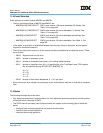
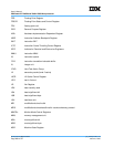
Table 11-7 shows the control bits for HID2.
The checkstop input pin (CKSTP_IN
) always causes a checkstop regardless of the state of the MSR[ME] bit.
Note: All checkstops are disabled by a hard reset. To enable the individual checkstops, the user has to set
the appropriate checking enable bits in HID0 and L2CR register.
11.9.3 Open-Collector-Driver States during Checkstop
All the nontest Open Collector Driver (OCD) states except for the checkstop output pin, CKSTP_OUT
, are
disabled during a checkstop. This forces the checkstopped processor off the bus, and prevents potential
OCD damage due to multiple drivers being enabled on the same bus during a checkstop.
11.9.4 Vacancy Slot Application
The checkstop input (CKSTP_IN
) to the 750GX can be used to implement a vacancy slot mechanism since a
checkstop halts the processor and tristates the OCDs as mentioned above. Several points need to be consid-
ered for the vacancy slot implementation:
• The internal checkstop logic requires its latches to be initialized properly upon a hard reset, and SYSCLK
to be running. Therefore, the processor that is being replaced needs to go through the same hard reset
sequence as the replacement processor. With SYSCLK running, the checkstop power consumption of the
750GX should be similar to the power consumption of the part in nap mode.
• Since a hard reset clears all checkstop conditions, the C
KSTP_IN pin needs to be kept asserted after the
negation of a hard reset for the part to enter checkstop.
• The checkstop output pin, CKSTP_OUT
, which is asserted, needs to be isolated.
• The IEEE 1149.1a-1993 requires the boundary scan output pin, TDO, to be controllable only by the JTAG
logic. Therefore, if the system POR sequence leaves the TDO pin tristated, then no further isolation is
required. However, if boundary scan is to be done with the replacement processor, then the JTAG logic of
the processor being replaced must be disabled through TRST
=0.
Table 11-7. HID2 Checkstop Control Bits
Bits Field Name
Hard
Reset
State
Description
29 ICPE Enable L1 instruction-cache or instruction-tag parity checking.
30 DCPE Enable L1 data-cache or data-tag parity checking.
31 L2PE Enable L2 Tag parity checking.
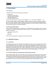
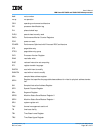
Table 11-8. L2CR Checkstop Control Bits
Bits
Field
Name
Hard
Reset
State
Description
22 SHEE 0
1 Enables a checkstop when snoop encounters a locked L2 line.
0 Prevents checkstop.
Enables a snoop hit in a locked line to raise a machine check. See Section 9.6.1.2,
Locked Cache Operation, on page 331 for more information.