


User’s Manual
IBM PowerPC 750GX and 750GL RISC Microprocessor
Bus Interface Operation
Page 282 of 377
gx_08.fm.(1.2)
March 27, 2006
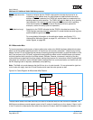
Cache lines are selected for replacement based on a pseudo least-recently-used (PLRU) algorithm. Each
time a cache line is accessed, it is tagged as the most-recently-used line of the set. When a miss occurs, and
all eight lines in the set are marked as valid, the least recently used line is replaced with the new data. When
data to be replaced is in the modified state, the modified data is written into a write-back buffer while the
missed data is being read from memory. When the load completes, the 750GX then pushes the replaced line
from the write-back buffer to the L2 cache (if enabled), or to main memory in a burst write operation.
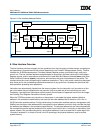
8.1.2 Operation of the Bus Interface
Memory accesses can occur in single-beat (1, 2, 3, 4, and 8 bytes) and 4-beat (32 bytes) burst data transfers.
The address and data buses are independent for memory accesses to support pipelining and split transac-
tions. The 750GX can pipeline as many as four load/store transactions and has limited support for out-of-
order split-bus transactions.
Access to the bus interface is granted through an external arbitration mechanism that allows devices to
compete for bus mastership. This arbitration mechanism is flexible, allowing the 750GX to be integrated into
systems that implement various fairness and bus-parking procedures to avoid arbitration overhead.
Typically, memory accesses are weakly ordered to maximize the efficiency of the bus without sacrificing
coherency of the data. The 750GX allows load operations to bypass store operations (except when a depen-
dency exists). In addition, the 750GX can be configured to reorder high-priority store operations ahead of
lower-priority store operations. Because the processor can dynamically optimize run-time ordering of
load/store traffic, overall performance is improved.
Note: The Synchronize (sync) and Enforce In-Order Execution of I/O (eieio) instructions can be used to
enforce strong ordering.
The following sections describe how the 750GX interface operates and provide detailed timing diagrams that
illustrate how the signals interact. A collection of more general timing diagrams are included as examples of
typical bus operations. Figure 8-2 on page 283 is a legend of the conventions used in the timing diagrams.
This is a synchronous interface—all 750GX input signals are sampled and output signals are driven on the
rising edge of the bus clock cycle (see the PowerPC 750GX Datasheet for exact timing information).
8.1.3 Bus Signal Clocking
All signals for the 750GX bus interface are specified with respect to the rising-edge of the external system
clock input (SYSCLK), and they are guaranteed to be sampled as inputs or changed as outputs with respect
to that edge.
System Implementation Note: Since the same clock edge is referenced for driving or sampling the bus sig-
nals, the possibility of clock skew exists between various modules in a system due to routing or the use of
multiple clock lines. It is the responsibility of the system to handle any such clock skew problems that could
occur.
8.1.4 Optional 32-Bit Data Bus Mode
The 750GX supports an optional 32-bit data bus mode. The 32-bit data bus mode operates the same as the
64-bit data bus mode with the exception of the byte lanes involved in the transfer and the number of data
beats that are performed. The number of data beats required for a data tenure in the 32-bit data bus mode is