User’s Manual
IBM PowerPC 750GX and 750GL RISC Microprocessor
gx_05.fm.(1.2)
March 27, 2006
Memory Management
Page 195 of 377
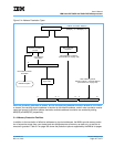
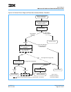
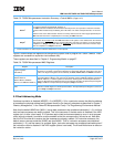
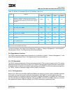
Figure 5-6 summarizes the registers that the operating system uses to program the 750GX’s MMUs. These
registers are accessible to supervisor-level software only.
These registers are described in Chapter 2, Programming Model, on page 57.
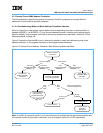
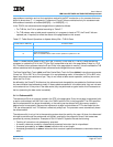
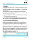
5.2 Real-Addressing Mode
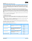
If address translation is disabled (MSR[IR] = 0 or MSR[DR] = 0) for a particular access, the effective address
is treated as the physical address and is passed directly to the memory subsystem as described in Chapter 7,
“Memory Management,” in the PowerPC Microprocessor Family: The Programming Environments Manual.
Note that the default WIMG bits (0b0011) cause data accesses to be considered cacheable (I = 0), and thus
load-and-store accesses are weakly ordered. This is the case even if the data cache is disabled in the HID0
register (as it is after a hard reset). If I/O devices require load-and-store accesses to occur in strict program
order (strongly ordered), translation must be enabled so that the corresponding I bit can be set. Note also,
that the G bit must be set to ensure that the accesses are strongly ordered. For instruction accesses, the
default memory-access mode bits (WIMG) are also 0b0001. That is, instruction accesses are considered
cacheable (I = 0), and the memory is guarded. Again, instruction accesses are considered cacheable even if
the instruction cache is disabled in the HID0 register (after a hard reset). The W and M bits have no effect on
the instruction cache.
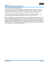
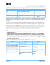
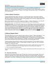
tlbie rB
1
TLB Invalidate Entry
For effective address specified by rB, TLB[V]
←0
The tlbie instruction invalidates all TLB entries indexed by the EA, and operates on both the instruction
and data TLBs simultaneously invalidating four TLB entries. The index corresponds to bits 14–19 of the
EA.
Software must ensure that instruction fetches or memory references to the virtual pages specified by the
tlbie instruction have been completed prior to executing the tlbie instruction.
tlbsync
1
TLB Synchronize
Synchronizes the execution of all other tlbie instructions in the system. In the 750GX, when the TLB Inval-
idate Synchronize (TLBISYNC
) signal is negated, instruction execution can continue or resume after the
completion of a tlbsync instruction. When the TLBISYNC
signal is asserted, instruction execution stops
after the completion of a tlbsync instruction.
1. These instructions are defined by the PowerPC Architecture, but are optional.
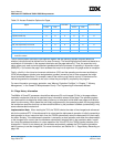
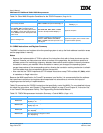
Table 5-6. 750GX Microprocessor MMU Registers
Register Description
Segment registers
(SR0–SR15)
The sixteen 32-bit Segment Registers are present only in 32-bit implementations of the PowerPC
Architecture. The fields in the Segment Register are interpreted differently depending on the value
of bit 0. The Segment Registers are accessed by the mtsr, mtsrin, mfsr, and mfsrin instructions.
BAT registers
(IBAT0U–IBAT7U,
IBAT0L–IBAT7L, DBAT0U–
DBAT7U, and DBAT0L–DBAT7L)
There are 32 BAT registers, organized as eight pairs of instruction BAT registers (IBAT0U–IBAT7U
paired with IBAT0L–IBAT7L) and eight pairs of data BAT registers (DBAT0U–DBAT7U paired with
DBAT0L–DBAT7L). The BAT registers are defined as 32-bit registers in 32-bit implementations.
These are Special-Purpose Registers that are accessed by the Move-to Special Purpose Register
(mtspr) and Move-from Special Purpose Register (mfspr) instructions.
SDR1
The SDR1 register specifies the variables used in accessing the page tables in memory. SDR1 is
defined as a 32-bit register for 32-bit implementations. This Special-Purpose Register is accessed
by the mtspr and mfspr instructions.
Table 5-5. 750GX Microprocessor Instruction Summary—Control MMUs (Page 2 of 2)
Instruction Description


