


User’s Manual
IBM PowerPC 750GX and 750GL RISC Microprocessor
Power and Thermal Management
Page 340 of 377
gx_10.fm.(1.2)
March 27, 2006
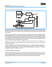
10.2.2 Power Management Software Considerations
Since the 750GX is a dual-issue processor with out-of-order execution capability, care must be taken in how
the power management mode is entered. Furthermore, nap and sleep modes require all outstanding bus
operations to be completed before these power management modes are entered. Normally, during system
configuration time, one of the power management modes would be selected by setting the appropriate HID0
mode bit. Later on, the power management mode is invoked by setting the MSR[POW] bit. To ensure a clean
transition into and out of a power management mode, the Move-to Machine State Register (mtmsr) (POW)
instruction should be preceded by a Synchronize (sync) instruction and followed by an Instruction Synchro-
nize (isync) as shown below.
...
loop:
sync
mtmsr (POW)
isync
br loop
...
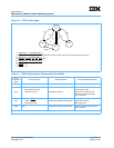
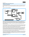
10.3 750GX Dual PLL Feature
10.3.1 Overview
Due to the relationship of power to frequency and voltage (power is proportional to frequency and a square of
voltage), running the processor at a lower frequency and associated lower voltage can result in significant
power savings. The 750GX design includes two PLLs (PLL0 and PLL1), which allows the processor clock
frequency to be dynamically changed to one of the PLL frequencies via software control. The HID1 Register
(described in Section 2.1.2.3 on page 70) contains fields that specify the frequency range of each PLL, the
clock multiplier for each PLL, external or internal control of PLL0, and a bit to choose which PLL is selected
(that is, which is the source of the processor clock at any given time). In addition, the supplied processor
voltage (V
DD
) can be varied to support the selected frequency: lower voltage, lower frequency, and lower
power for normal processing tasks or higher voltage, higher frequency for situations requiring high perfor-
mance. PLL voltages (AV
DD
) should remain constant at all times.
At power-on reset, the HID1 Register contains zeros for all the non-read-only bits (bits 7 to 31). This configu-
ration corresponds to the selection of PLL0 as the source of the processor clocks, and selects the external
configuration and range pins to control PLL0 (see Chapter 8, Bus Interface Operation, on page 279). The
external configuration and range pin values are accessible to software via HID1 read-only bits 0-6. PLL1 is
always controlled by its internal configuration and range bits. The HID1 setting associated with a hard reset
corresponds to a PLL1 configuration of clock off, and the selection of the medium frequency range.
As stated in the PowerPC 750GX RISC Microprocessor Datasheet, HRESET
must be asserted during power
up long enough for the PLLs to lock and for the internal hardware to be reset. Once this timing is satisfied,
HRESET
can be negated. The processor will now proceed to execute instructions, clocked by PLL0 as
configured via the external pins. The processor clock frequency can be modified from this initial setting in one
of two ways. First, as with earlier designs, HRESET
can be asserted, and the external configuration pins can
be set to a new value. The machine state is lost in this process, and, as always, HRESET
must be held
asserted while the PLL relocks, and the internal state is reset. Second, the introduction of another PLL
provides an alternative means of changing the processor clock frequency, which does not involve the loss of
machine state, nor a delay for PLL relock.