


User’s Manual
IBM PowerPC 750GX and 750GL RISC Microprocessor
gx_07.fm.(1.2)
March 27, 2006
Signal Descriptions
Page 277 of 377
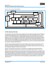
7.2.15.1 System Clock (SYSCLK)—Input
The 750GX requires a single system clock (SYSCLK) input. This input sets the frequency of operation for the
bus interface. Internally, the 750GX uses a PLL circuit to generate a master clock for all of the CPU circuitry
(including the bus interface circuitry) which is phase-locked to the SYSCLK input.
7.2.15.2 Clock Out (CLK_OUT)—Output
The clock out (CLK_OUT) signal is an output signal.
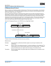
7.2.15.3 PLL Configuration (PLL_CFG[0:4])—Input
The PLL is configured by the PLL_CFG[0:4] signals. For a given SYSCLK (bus) frequency, the PLL configu-
ration signals set the internal CPU frequency of operation. See the PowerPC 750GX Datasheet for PLL
configuration.
State Asserted/
Negated
The primary clock input for the 750GX. SYSCLK represents the bus clock
frequency for bus operation. Internally, the processor core will be operating
at an integer or half-integer multiple (≥ 1.0) of the bus clock frequency.
Timing Assertion/
Negation
See the IBM PowerPC 750GX RISC Microprocessor Datasheet for timing
comments. Loose duty cycle allowed.
Note: SYSCLK is used as a frequency reference for the internal PLL clock
regenerator. It must not be suspended or varied during normal operation to
ensure proper PLL operation.
State Asserted/
Negated
PLL clock output for PLL testing or monitoring. (See HID1 for select and
enable.)
The CLK_OUT signal is provided for testing only.
Timing Assertion/
Negation
See the IBM PowerPC 750GX RISC Microprocessor Datasheet. Driven with
a bus-rate clock during the assertion of HRESET
. The default state during
normal operation is high impedance.
State Asserted/
Negated
Configures the operation of the PLL and the internal processor clock
frequency. Settings are based on the desired bus and internal frequency of
operation.
Timing Assertion/
Negation
Must remain stable during operation; should only be changed during the
assertion of HRESET
. These bits can be read through the PCE[0–4] bits in
the HID1 register.