


User’s Manual
IBM PowerPC 750GX and 750GL RISC Microprocessor
Signal Descriptions
Page 254 of 377
gx_07.fm.(1.2)
March 27, 2006
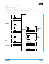
7.2.3 Address Transfer Signals
The address transfer signals are used to transmit the address and to generate and monitor parity for the
address transfer. For a detailed description of how these signals interact, see Section 8.3.2, Address
Transfer, on page 292.
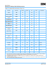
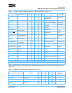
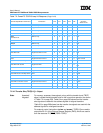
7.2.3.1 Address Bus (A[0–31])
The address bus (A[0–31]) consists of 32 signals that are both input and output signals.
Address Bus (A[0–31])—Output
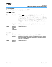
Address Bus (A[0–31])—Input
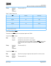
State Asserted/
Negated
Represents the physical address (real address in the architecture specifica-
tion) of the data to be transferred. On burst transfers, the address bus
presents the double-word-aligned address containing the critical code/data
that missed the cache on a read operation, or the first double word of the
cache line on a write operation. Note that the address output during burst
operations is not incremented. See Section 8.3.2, Address Transfer, on
page 292.
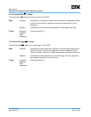
Timing Assertion/
Negation
Occurs on the bus clock cycle after a qualified bus grant (coincides with
assertion of TS
). Remains driven/valid for the duration of the address tenure.
High
Impedance
Occurs one bus clock cycle following the assertion of AACK
; no precharge
action is performed on release.
State Asserted/
Negated
Represents the physical address of a snoop operation.
Timing Assertion/
Negation
Must occur on the same bus clock cycle as the assertion of TS
; is sampled by
the 750GX only on this cycle.