


User’s Manual
IBM PowerPC 750GX and 750GL RISC Microprocessor
PowerPC 750GX Overview
Page 24 of 377
gx_01.fm.(1.2)
March 27,2006
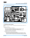
and data block-address-translation (IBAT and DBAT) arrays, defined by the PowerPC Architecture. During
block translation, effective addresses are compared simultaneously with all eight block-address-translation
(BAT) entries.
For information about the L1 cache, see Chapter 3, Instruction-Cache and Data-Cache Operation, on
page 121. The L2 cache is implemented with an on-chip, 4-way set-associative tag memory, and an on-chip
1-MB SRAM with error correction code (ECC) protection for data storage. For more information on the L2
Cache, see Chapter 9 on page 323.
The 750GX has a 32-bit address bus and a 64-bit data bus. Multiple devices compete for system resources
through a central external arbiter. The 750GX’s 3-state cache-coherency protocol (MEI) supports the modi-
fied, exclusive, and invalid states, a compatible subset of the MESI (modified/exclusive/shared/invalid)
4-state protocol, and it operates coherently in systems with 4-state caches. The 750GX supports single-beat
and burst data transfers for external memory accesses and memory-mapped I/O operations. The system
interface is described in Chapter 7, Signal Descriptions, on page 249 and Chapter 8, Bus Interface Opera-
tion, on page 279.
The 750GX has four software-controllable power-saving modes. The three static modes; doze, nap, and
sleep; progressively reduce power dissipation. When functional units are idle, a dynamic power management
mode causes those units to enter a low-power mode automatically without affecting operational performance,
software execution, or external hardware. The 750GX also provides a thermal assist unit (TAU) and a way to
reduce the instruction fetch rate to limit power dissipation. Power management is described in Chapter 10,
Power and Thermal Management, on page 335.