


User’s Manual
IBM PowerPC 750GX and 750GL RISC Microprocessor
gx_07.fm.(1.2)
March 27, 2006
Signal Descriptions
Page 267 of 377
Data Bus (DH[0–31], DL[0–31])—Output
Data Bus (DH[0–31], DL[0–31])—Input
7.2.7.2 Data-Bus Parity (DP[0–7])
The eight data-bus parity (DP[0–7]) signals are both input and output signals.
Data-Bus Parity (DP[0–7])—Output
State Asserted/
Negated
Represents the state of data during a data write. For single-beat (cache
inhibited or write through) writes, byte lanes not selected for data transfer will
not supply valid data (no data mirroring).
Timing Assertion/
Negation
First or only beat begins on the cycle of DBB
assertion and, for bursts, tran-
sitions on the cycle following each initially qualified assertion of TA
.
High
Impedance
Occurs on the bus clock cycle after the final assertion of TA
, following the
assertion of TEA
, or in certain ARTRY cases.
State Asserted/
Negated
Represents the state of data during a data read transaction.
Timing Assertion/
Negation
Data must be valid on the same bus clock cycle that TA
is asserted, even if
during the last assertion cycle of DRTRY
.
State Asserted/
Negated
Represents odd parity for each of the 8 bytes of data write transactions. Odd
parity means that an odd number of bits, including the parity bit, are driven
high. The generation of parity is enabled through HID0. The signal assign-
ments are listed in Table 7-5.
Timing Assertion/
Negation/
High
Impedance
The same as DL[0–31].
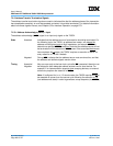
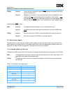
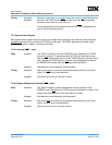
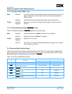
Table 7-5. DP[0–7] Signal Assignments
Signal Name Signal Assignments
DP0 DH[0–7]
DP1 DH[8–15]
DP2 DH[16–23]
DP3 DH[24–31]
DP4 DL[0–7]
DP5 DL[8–15]
DP6 DL[16–23]
DP7 DL[24–31]