


User’s Manual
IBM PowerPC 750GX and 750GL RISC Microprocessor
gx_07.fm.(1.2)
March 27, 2006
Signal Descriptions
Page 255 of 377
7.2.3.2 Address-Bus Parity (AP[0–3])
The address-bus parity (AP[0–3]) signals are both input and output signals reflecting 1 bit of odd-byte parity
for each of the 4 bytes of address when a valid address is on the bus.
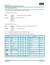
Address-Bus Parity (AP[0–3])—Output
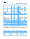
Address-Bus Parity (AP[0–3])—Input
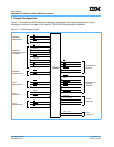
7.2.4 Address Transfer Attribute Signals
The transfer attribute signals are a set of signals that further characterize the transfer—such as the size of the
transfer, whether it is a read or write operation, and whether it is a burst or single-beat transfer. For a detailed
description of how these signals interact, see Section 8.3.2, Address Transfer, on page 292.
Note: Some signal functions vary depending on whether the transaction is a memory access or an I/O
access.
State Asserted/
Negated
Represents odd parity for each of the 4 bytes of the physical address for a
transaction. Odd parity means that an odd number of bits, including the
parity bit, are driven high. Address parity is generated by the 750GX as
address-bus master (unless disabled through Hardware-Implementation-
Dependent Register 0 [HID0]). The signal assignments correspond to the
following:
AP0 A[0–7]
AP1 A[8–15]
AP2 A[16–23]
AP3 A[24–31]
Timing Assertion/
Negation/
High
Impedance
The same as A[0–31].
State Asserted/
Negated
Represents odd parity for each of the 4 bytes of the physical address for
snooping operations. Detected even parity causes the processor to take a
machine check exception or enter the checkstop state if address-parity
checking is enabled in the HID0 register. See Section 2.1.2.2, Hardware-
Implementation-Dependent Register 0 (HID0), on page 65.
Timing Assertion/
Negation
The same as A[0–31].