


User’s Manual
IBM PowerPC 750GX and 750GL RISC Microprocessor
Signal Descriptions
Page 266 of 377
gx_07.fm.(1.2)
March 27, 2006
Data Bus Busy (DBB)—Input
7.2.7 Data-Transfer Signals
Like the address transfer signals, the data-transfer signals are used to transmit data and to generate and
monitor parity for the data transfer. For a detailed description of how the data-transfer signals interact, see
Section 8.4.3, Data Transfer, on page 303. Data parity is optional on the 750GX.
7.2.7.1 Data Bus (DH[0–31], DL[0–31])
The data bus (DH[0–31] and DL[0–31]) consists of 64 signals that are both inputs and outputs on the 750GX.
Timing Assertion Occurs the cycle following a qualified DBG
. Remains asserted for the dura-
tion of the data tenure.
Negation Negates for a fraction of a bus cycle (one-half minimum, depends on clock
mode) starting the cycle following the final assertion of the transfer
acknowledge (TA
) signal, or following the transfer error acknowledge (TEA)
signal or certain ARTRY
cases. Then releases to the high impedance state.
State Asserted Indicates that another master is the current data-bus owner.
Negated Indicates that the data bus might be available for use by the 750GX (see
DBG
).
Timing Assertion May occur when the 750GX must be prevented from using the data bus.
Negation May occur whenever the 750GX can use the data bus.
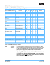
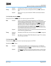
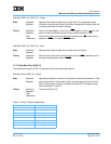
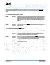
State The data bus has two halves—data bus high (DH) and data bus low (DL). See Table 7-4 on
page 266 for the data-bus lane assignments.
Timing The data bus is driven once for noncached transactions and four times for cache transac-
tions (bursts).
Table 7-4. Data-Bus Lane Assignments
Data-Bus Signals Byte Lane
DH[0–7] 0
DH[8–15] 1
DH[16–23] 2
DH[24–31] 3
DL[0–7] 4
DL[8–15] 5
DL[16–23] 6
DL[24–31] 7