


User’s Manual
IBM PowerPC 750GX and 750GL RISC Microprocessor
gx_05.fm.(1.2)
March 27, 2006
Memory Management
Page 181 of 377
5.1.1 Memory Addressing
A program references memory using the effective (logical) address computed by the processor when it
executes a load, store, branch, or cache instruction, and when it fetches the next instruction. The effective
address is translated to a physical address according to the procedures described in Chapter 7, “Memory
Management” in the PowerPC Microprocessor Family: The Programming Environments Manual, augmented
with information in this section. The memory subsystem uses the physical address for the access.
For a discussion of effective address calculation, see Section 2.3.2.3 on page 90.
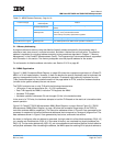
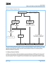
5.1.2 MMU Organization
Figure 5-1, MMU Conceptual Block Diagram, on page 183 shows the conceptual organization of a PowerPC
MMU in a 32-bit implementation. However, it does not describe the specific hardware used to implement the
memory-management function for a particular processor. Processors might optionally implement on-chip
TLBs, hardware support for the automatic search of the page tables for PTEs, and other hardware features
(invisible to the system software) that are not shown.
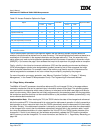
The 750GX maintains two on-chip TLBs with the following characteristics:
• 128 entries, 2-way set associative (64 × 2), LRU replacement
• Data TLB supports the DMMU; instruction TLB supports the IMMU
• Hardware TLB update
• Hardware update of referenced (R) and changed (C) bits in the translation table
In the event of a TLB miss, the hardware attempts to load the TLB based on the results of a translation table-
search operation.
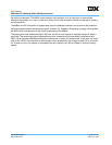
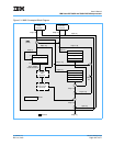
Figure 5-2, PowerPC 750GX Microprocessor IMMU Block Diagram, on page 184 and Figure 5-3, 750GX
Microprocessor DMMU Block Diagram, on page 185 show the conceptual organization of the 750GX’s
instruction and data MMUs, respectively. The instruction addresses shown in Figure 5-2 are generated by the
processor for sequential instruction fetches and addresses that correspond to a change of program flow. The
data addresses shown in Figure 5-3 are generated by load, store, and cache instructions.
As shown in the figures, after an address is generated, the high-order bits of the effective address, EA[0–19]
(or a smaller set of address bits, EA[0–n], in the cases of blocks), are translated into physical address bits
PA[0–19]. The low-order address bits, A[20–31], are untranslated and are therefore identical for both effective
and physical addresses. After translating the address, the MMUs pass the resulting 32-bit physical address to
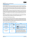
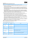
TLBs
Architecturally defined
Instructions for maintaining TLBs (tlbie and tlbsync instructions in the
750GX)
750GX-specific
128-entry, 2-way set-associative ITLB
128-entry, 2-way set-associative DTLB
Least recently used (LRU) replacement algorithm
Segment descriptors Architecturally defined Stored as segment registers on-chip (two identical copies maintained)
Page table-search support 750GX-specific The
750GX performs the table-search operation in hardware.
Table 5-1. MMU Feature Summary (Page 2 of 2)
Feature Category
Architecturally Defined/
750GX-Specific
Feature