


User’s Manual
IBM PowerPC 750GX and 750GL RISC Microprocessor
gx_08.fm.(1.2)
March 27, 2006
Bus Interface Operation
Page 309 of 377
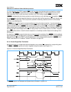
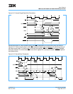
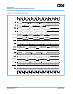
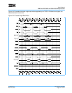
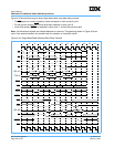
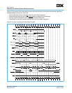
8.5 Timing Examples
This section shows timing diagrams for various scenarios. Figure 8-17 on page 310 illustrates the fastest
single-beat reads possible for the 750GX. This figure shows both minimal latency and maximum single-beat
throughput. By delaying the data-bus tenure, the latency increases, but, because of split-transaction pipe-
lining, the overall throughput is not affected unless the data-bus latency causes the third address tenure to be
delayed.
Note that all bidirectional signals are tristated between bus tenures.
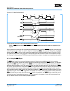
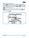
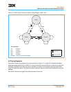
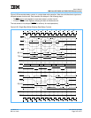
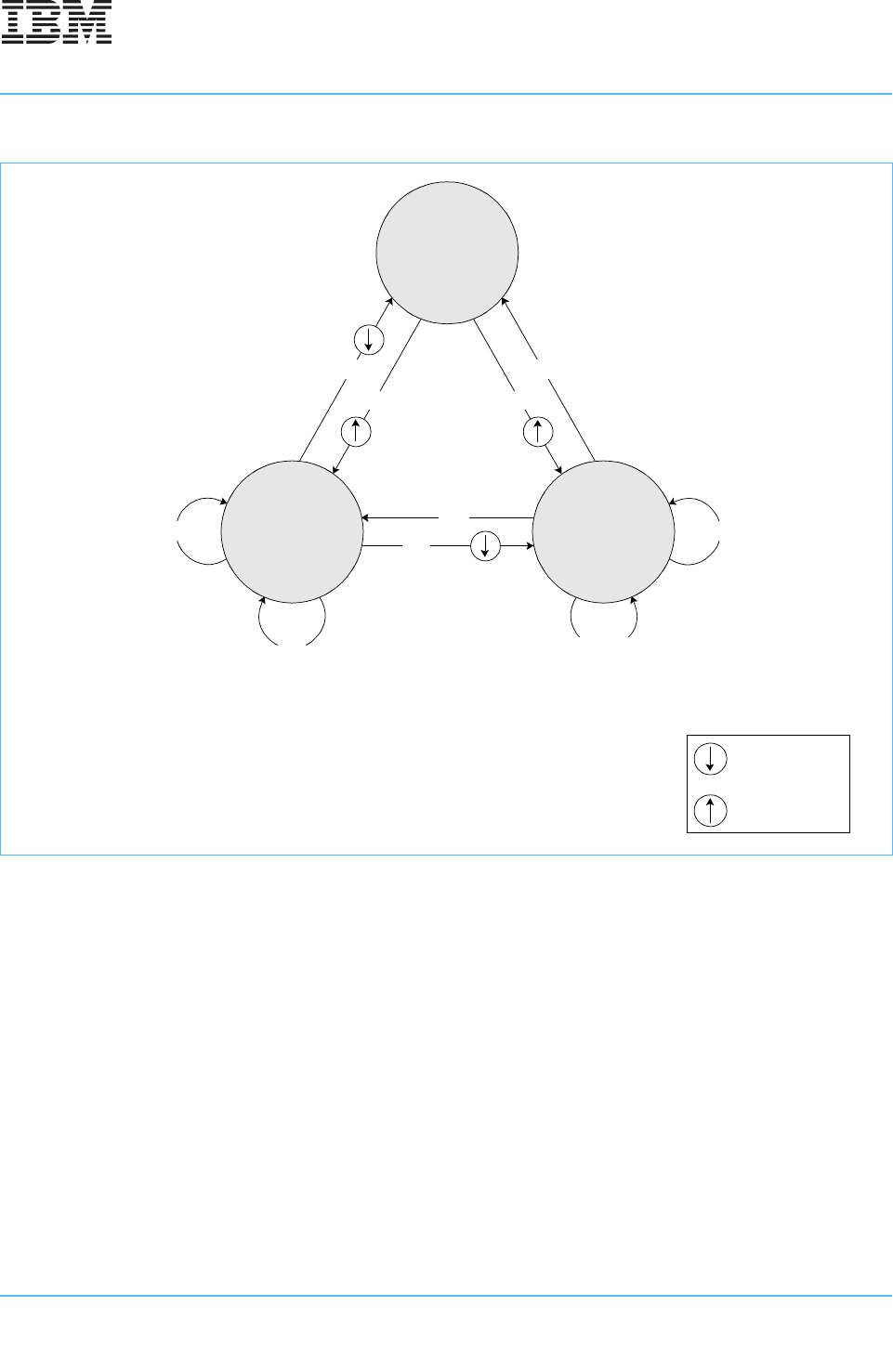
Figure 8-16. MEI Cache-Coherency Protocol—State Diagram (WIM = 001)
Bus Transactions
SH = Snoop Hit
RH = Read Hit
RM = Read Miss
WH = Write Hit
WM = Write Miss
SH/CRW = Snoop Hit, Cacheable Read/Write
SH/CRW
WM RM
SH/CRW
Invalid
ExclusiveModified
RH RH
SH/CIRWH
WH
SH
Snoop Push
Cache Block Fill