


User’s Manual
IBM PowerPC 750GX and 750GL RISC Microprocessor
Signal Descriptions
Page 276 of 377
gx_07.fm.(1.2)
March 27, 2006
7.2.14.3 L1_TSTCLK
7.2.14.4 L2_TSTCLK
7.2.14.5 BVSEL
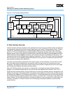
7.2.15 Clock Signals
The 750GX requires a single system clock input (SYSCLK). This input represents the frequency at which the
bus interface for the 750GX will operate. Internally, the 750GX uses a PLL circuit to generate a master core
clock that is frequency-multiplied and phase-locked to the SYSCLK input. This master core clock is the clock
actually used by the 750GX to operate the internal circuitry. The PLL samples the master clock at the latch
boundary (that is, end of clock tree) and minimizes the clock skew between the rising edge of SYSCLK and
the master clock at the latch boundary. This mechanism provides I/O timings accurate to the rising edge of
SYSCLK. However, if the chip is operated in bypass mode (PLL not used), this phase correcting circuitry
cannot be used, and the I/O timings are unreliable.
The PLL is configured by the PLL_CFG(0:4) pins. These pins select the multiplier that the PLL will use to
multiply the SYSCLK frequency up to the internal core frequency. In addition, the pins PLL_RNG(0:1) must
be set to select the appropriate frequency operating range of the PLL. See the PowerPC 750GX Datasheet
for more information.
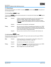
State LSSD test clock in test mode, and bus voltage select in functional mode. See
Table 7-7, Bus Voltage Selection Settings, on page 275.
Timing Assertion/
Negation
Signal should be held to a constant value for I/O voltage selection.
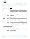
State Reserved pin that must be negated for system operation.
Timing Assertion/
Negation
Must be held constant for system operation.
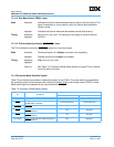
Start-Up See Table 7-6, Summary of Mode Select Signals, on page 274 for a descrip-
tion of the start-up function.
State I/O voltage is selectable through using the BVSEL pin and L1_TSTCLK pin.
See Table 7-7, Bus Voltage Selection Settings, on page 275.
Timing Signal should be held to a constant value for I/O voltage selection.