


User’s Manual
IBM PowerPC 750GX and 750GL RISC Microprocessor
gx_09.fm.(1.2)
March 27, 2006
L2 Cache
Page 323 of 377
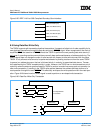
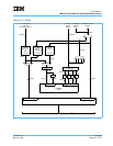
9. L2 Cache
This chapter describes the 750GX microprocessor‘s implementation of the 1-MB L2 cache.
Note: The L2 cache is initially disabled following a power-on or hard reset. Before enabling the L2 cache,
configuration parameters must be set in the L2 Cache Control Register (L2CR), and the L2 tags must be
globally invalidated. The L2 cache should be initialized during system start-up (see Section 9.4 on page 329).
9.1 L2 Cache Overview
The 750GX microprocessor’s L2 cache is implemented with an internal 4-way set-associative tag memory
with 4096 tags per way, and an internal 1-MB SRAM for data storage. The tags are sectored to support two
cache blocks per tag entry (two 32-byte sectors totalling 64 bytes). Each sector (32-byte cache block) in the
L2 cache has its own valid and modified bits. Each set of four cache lines maintains three least recently used
(LRU) bits to implement a pseudo-LRU replacement mechanism. In addition, the SRAM includes an 8-bit
error correction code (ECC) for every double word. The ECC logic corrects most single-bit errors and detects
the remaining single-bit errors and all double-bit errors as data is read from the SRAM. The L2 cache main-
tains cache coherency through snooping, and is normally configured to operate in copy-back mode.
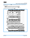
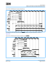
The L2 Cache Control Register (L2CR) allows control of the following:
• L2-cache configuration
• Double-bit error machine check
• Global invalidation of L2 contents
• Write-through operation
• L2 test support
• L2 locking by way
• Data-only and instruction-only modes
9.2 L2 Cache Operation
The L2 cache for the 750GX microprocessor is a combined instruction and data cache that receives memory
requests from both L1 instruction and L1 data caches independently. The L1 requests are generally the result
of instruction fetch misses, data load or store misses, write-through operations, or cache-management
instructions. Each L1 request generates an address lookup in the L2 tags. If a hit occurs, the instructions or
data are forwarded to the L1 cache. A miss in the L2 tags causes the L1 request to be forwarded to the 60x
bus interface. The cache block received from the bus is forwarded to the L1 cache immediately, and is also
loaded into the L2 cache with the tag marked valid and unmodified. If the cache block loaded into the L2
cache causes a new tag entry to be allocated and the current tag entry is marked valid modified, the modified
sectors of the tag to be replaced are castout from the L2 cache to the 60x bus.
At any given time, the L1 instruction cache might have one instruction fetch request, and the L1 data cache
might have four loads and two stores requesting L2 cache access. The L2 cache also services snoop
requests from the 60x bus. When there are multiple pending requests to the L2 cache, snoop requests have
highest priority, followed by data load-and-store requests (serviced on a first-in, first-out basis). Instruction
fetch requests have the lowest priority in accessing the L2 cache when there are multiple accesses pending.