


User’s Manual
IBM PowerPC 750GX and 750GL RISC Microprocessor
gx_03.fm.(1.2)
March 27, 2006
Instruction-Cache and Data-Cache Operation
Page 139 of 377
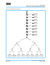
The data-cache flush assist bit, HID0[DCFA], simplifies the software flushing process. When set,
HID0[DCFA] forces the PLRU replacement algorithm to ignore the invalid entries and follow the replacement
sequence defined by the PLRU bits. This reduces the series of uniquely addressed load or dcbz instructions
to eight per set. HID0[DCFA] should be set just prior to the beginning of the cache flush routine and cleared
after the series of instructions is complete.
The L2 flush mechanism is similar to the L1 data-cache flush mechanism. The L2 flush requires that the
entire data cache be flushed prior to flushing the L2 cache. Also, exceptions must be disabled during the L2
flush so that the LR and PLRU algorithms are not disturbed. The L2 cache can be flushed by executing
uniquely addressed load instructions to each of the 32-byte blocks of the L2 cache. This can be done by
loading a contiguous 1-MB block of memory. The loads must not hit in the L1 cache in order to effect a flush
of the L2 cache.
3.5.3 Data-Cache Block-Fill Operations
The 750GX’s data-cache blocks are filled in four beats of 64 bits each, with the critical double word loaded
first. The data cache is not blocked to internal accesses while the load (caused by a cache miss) completes.
This functionality is sometimes referred to as ‘hits under misses,’ because the cache can service a hit while a
cache miss fill is waiting to complete. The critical-double-word read from memory is simultaneously written to
the data cache and forwarded to the requesting unit, thus minimizing stalls due to cache fill latency.
A cache block is filled after a read miss or write miss (read-with-intent-to-modify) occurs in the cache. The
cache block that corresponds to the missed address is updated by a burst transfer of the data from the L2 or
system memory. Note that if a read miss occurs in a system with multiple bus masters, and the data is modi-
fied in another cache, the modified data is first written to external memory before the cache fill occurs.
3.5.4 Instruction-Cache Block-Fill Operations
The 750GX’s instruction-cache blocks are loaded in four beats of 64 bits each, with the critical double word
loaded first. The instruction cache is not blocked to internal accesses while the fetch (caused by a cache
miss) completes. On a cache miss, the critical and following double words read from memory are simulta-
neously written to the instruction cache and forwarded to the instruction queue, thus minimizing stalls due to
cache fill latency. There is no snooping of the instruction cache.
3.5.5 Data-Cache Block-Push Operations
When a cache block in the 750GX is snooped and hit by another bus master and the data is modified, the
cache block must be written to memory and made available to the snooping device. The cache block is said
to be pushed out onto the 60x bus.
3.6 L1 Caches and 60x Bus Transactions
The 750GX transfers data to and from the cache in single-beat transactions of two words, or in 4-beat trans-
actions of eight words which fill a cache block. Single-beat bus transactions can transfer from one to eight
bytes to or from the 750GX, and can be misaligned. Single-beat transactions can be caused by cache write-
through accesses, caching-inhibited accesses (WIMG = x1xx), accesses when the cache is disabled
(HID0[DCE] bit is cleared), or accesses when the cache is locked (HID0[DLOCK] bit is cleared).