


User’s Manual
IBM PowerPC 750GX and 750GL RISC Microprocessor
Programming Model
Page 70 of 377
gx_02.fm.(1.2)
March 27, 2006
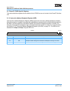
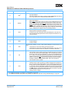
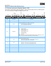
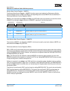
2.1.2.3 Hardware-Implementation-Dependent Register 1 (HID1)
The Hardware-Implementation-Dependent Register 1 (HID1) reflects the state of the PLL_CFG[0:4] signals.
HID1 can be accessed with mtspr and mfspr using SPR 1009.
PCE PRE
PSTAT1
ECLK
Reserved
Reserved
PI0
PS PC0 PR0
Reserved
PC1 PR1
Reserved
012345678910111213141516171819202122232425262728293031
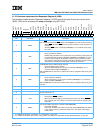
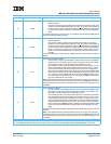
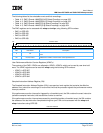
Bits Field Name Description
0:4 PCE PLL external configuration bits (read-only).
5:6 PRE PLL external range bits (read-only).
7PSTAT1
PLL status. Specifies the PLL clocking the processor:
0 PLL0 is the processor clock source
1 PLL1 is the processor clock source.
8 ECLK Set to 1 to enable the CLKOUT pin.
9:11 Reserved
Select the internal clock to be output on the CLKOUT pin with the following decode:
000 Factory use only
001 PLL0 core clock (freq/2)
010 Factory use only
011 PLL1 core clock (freq/2)
100 Factory use only
101 Core clock (freq/2)
Other Reserved
Note: These clock configuration bits reflect the state of the PLL_CFG[0:4] pins. Clock
options should only be used for design debug and characterization.
12:13 Reserved Reserved.
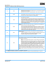
14 PI0
PLL 0 internal configuration select.
0 Select external configuration and range bits to control PLL 0.
1 Select internal fields in HID1 to control PLL0.
15 PS
PLL select.
0 Select PLL 0 as the source for the processor clock.
1 Select PLL 1 as the source for the processor clock.
16:20 PC0 PLL 0 configuration bits.
21:22 PR0 PLL 0 range select bits.
23 Reserved Reserved.
24:28 PC1 PLL 1 configuration bits.
29:30 PR1 PLL 1 range bits.
31 Reserved Reserved.