


User’s Manual
IBM PowerPC 750GX and 750GL RISC Microprocessor
gx_01.fm.(1.2)
March 27,2006
PowerPC 750GX Overview
Page 47 of 377
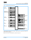
1.5.2 750GX Microprocessor Instruction Set
750GX instruction set is defined as follows.
• 750GX provides hardware support for all PowerPC instructions.
• 750GX implements the following instructions, which are optional in the PowerPC Architecture.
– External Control In Word Indexed (eciwx).
– External Control Out Word Indexed (ecowx).
– Floating Select (fsel).
– Floating Reciprocal Estimate Single-Precision (fres).
– Floating Reciprocal Square Root Estimate (frsqrte).
– Store Floating-Point as Integer Word (stfiw).
Note: The fres and frsqrte instructions are implemented in the 750GX with 12-bit precision (better than one
part in 4000), which significantly exceeds the minimum precision required by the architecture.
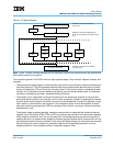
1.6 On-Chip Cache Implementation
The following subsections describe the PowerPC Architecture’s treatment of cache in general, and the
750GX-specific implementation. A detailed description of the 750GX L1 cache implementation is provided in
Chapter 3, Instruction-Cache and Data-Cache Operation, on page 121. A detailed description of the L2 cache
is provided in Chapter 9, L2 Cache, on page 323.
1.6.1 PowerPC Cache Model
The PowerPC Architecture does not define hardware aspects of cache implementations. For example,
PowerPC processors can have unified caches, separate instruction and data caches (Harvard architecture),
or no cache at all. PowerPC microprocessors control the following memory-access modes on a virtual-page
or block (BAT) basis
• Write-back/write-through mode
• Caching-inhibited mode
• Memory coherency
The caches are physically addressed, and the data cache can operate in either write-back or write-through
mode, as specified by the PowerPC Architecture.
The PowerPC Architecture defines the term ‘cache block’ as the cacheable unit. The VEA and OEA define
cache-management instructions that a programmer can use to affect cache contents.
1.6.2 750GX Microprocessor Cache Implementation
750GX cache implementation is described in Section 1.2.4, On-Chip Level 1 Instruction and Data Caches, on
page 33 and Section 1.2.5, On-Chip Level 2 Cache Implementation, on page 35.
The BPU also contains a cache, the 64-entry BTIC, that provides immediate access to an instruction pair for
taken branches. For more information, see Section 1.2.1.2, Branch Processing Unit (BPU), on page 29.