


Rev.1.10 Jul 01, 2005 page 92 of 318
REJ09B0124-0110
M16C/6N Group (M16C/6NK, M16C/6NM) 12. Timers
Under development
This document is under development and its contents are subject to change.
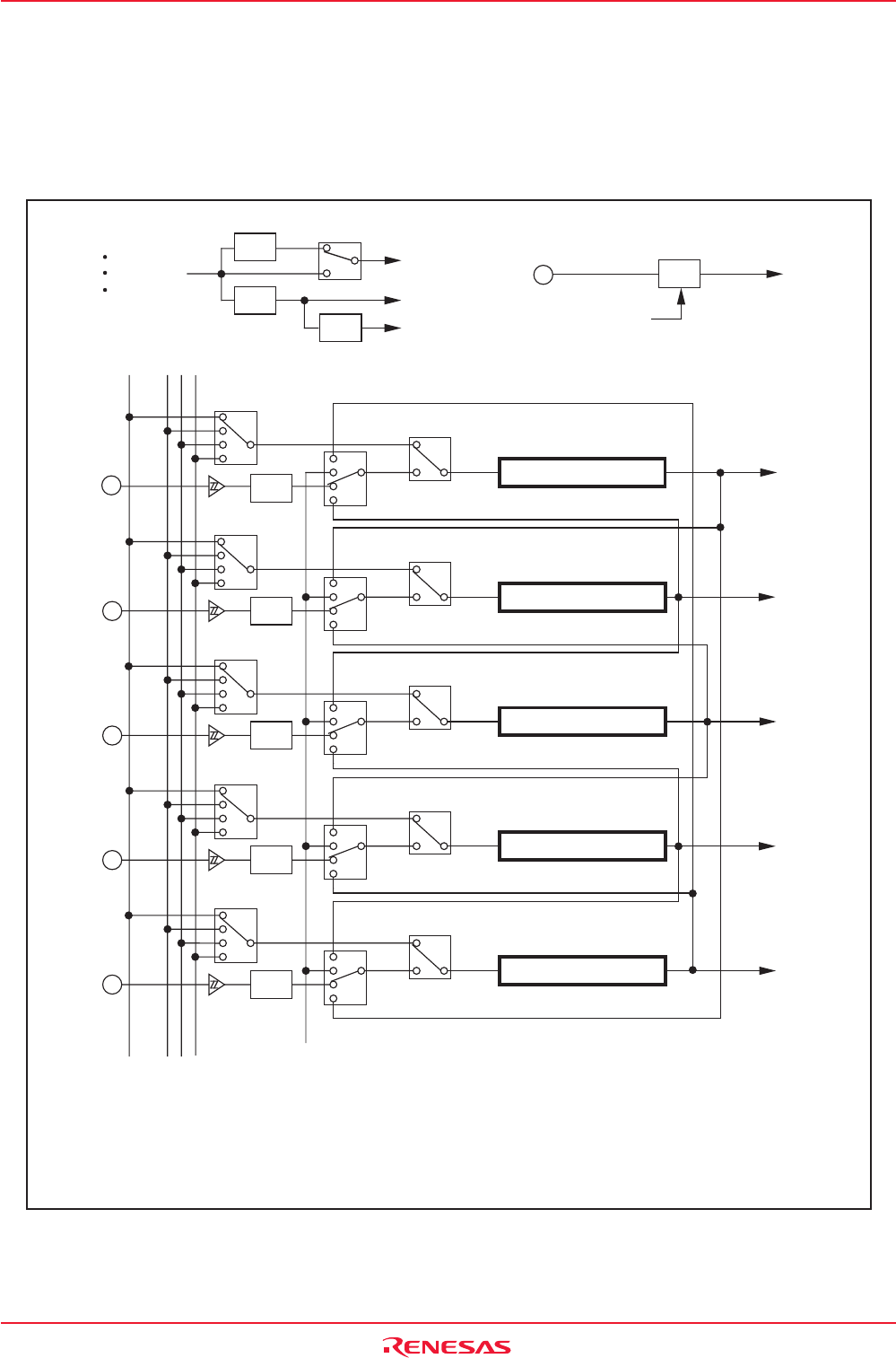
12. Timers
Eleven 16-bit timers, each capable of operating independently of the others, can be classified by function as
either timer A (five) and timer B (six). The count source for each timer acts as a clock, to control such timer
operations as counting, reloading, etc.
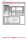
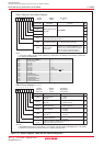
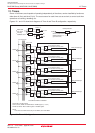
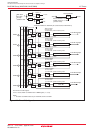
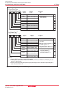
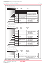
Figures 12.1 and 12.2 show block diagrams of Timer A and Timer B configuration, respectively.
TA0IN
TA1IN
TA2IN
TA3IN
TA4IN
Timer A0
Timer A1
Timer A2
Timer A3
Timer A4
f1 or f2 f8 f32 fC32
Timer A0 interrupt
Timer A1 interrupt
Timer A2 interrupt
Timer A3 interrupt
Timer A4 interrupt
Noise
filter
Noise
filter
Noise
filter
Noise
filter
Timer B2 overflow or underflow
PCLK0: Bit in PCLKR register
TCK1 to TCK0, TMOD1 to TMOD0: Bits in TAiMR register (i = 0 to 4)
TAiTGH to TAiTGL: Bits in ONSF register or TRGSR register
NOTE:
1. Be aware that TA0IN shares the pin with RXD2, SCL2 and TB5IN.
TCK1 to TCK0
10
01
00
11
00
01
10
11
00
01
10
11
00
01
10
11
00
01
10
11
00
01
10
11
TA0TGH to TA0TGL
TMOD1 to TMOD0 00:
Timer mode
10 :
One-shot timer mode
11 :
Pulse width measuring mode
01:
Event counter mode
TMOD1 to TMOD0 00:
Timer mode
10 :
One-shot timer mode
11 :
Pulse width measuring mode
01:
Event counter mode
TMOD1 to TMOD0 00:
Timer mode
10 :
One-shot timer mode
11 :
Pulse width measuring mode
01:
Event counter mode
TMOD1 to TMOD0 00:
Timer mode
10 :
One-shot timer mode
11 :
Pulse width measuring mode
01:
Event counter mode
TMOD1 to TMOD0 00:
Timer mode
10 :
One-shot timer mode
11 :
Pulse width measuring mode
01:
Event counter mode
TCK1 to TCK0
TCK1 to TCK0
TCK1 to TCK0
TCK1 to TCK0
10
01
00
11
TA1TGH t0 TA1TGL
10
01
00
11
TA2TGH to TA2TGL
10
01
00
11
TA3TGH to TA3TGL
10
01
00
11
TA4TGH to TA4TGL
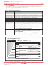
1/32
fC32
XCIN
Reset
Clock prescaler
Set the CPSR bit in the
CPSRF register to "1"
(prescaler reset)
1/8
1/4
f1 or f2
f8
f32
1/2
f1
f2
PCLK0 = 0
PCLK0 = 1
Main clock
PLL clock
On-chip
oscillator clock
Noise
filter
Figure 12.1 Timer A Configuration