


Rev.1.10 Jul 01, 2005 page 232 of 318
REJ09B0124-0110
M16C/6N Group (M16C/6NK, M16C/6NM) 19. Programmable I/O Ports
Under development
This document is under development and its contents are subject to change.
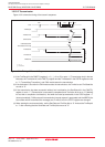
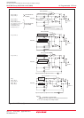
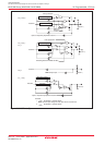
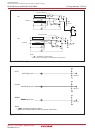
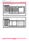
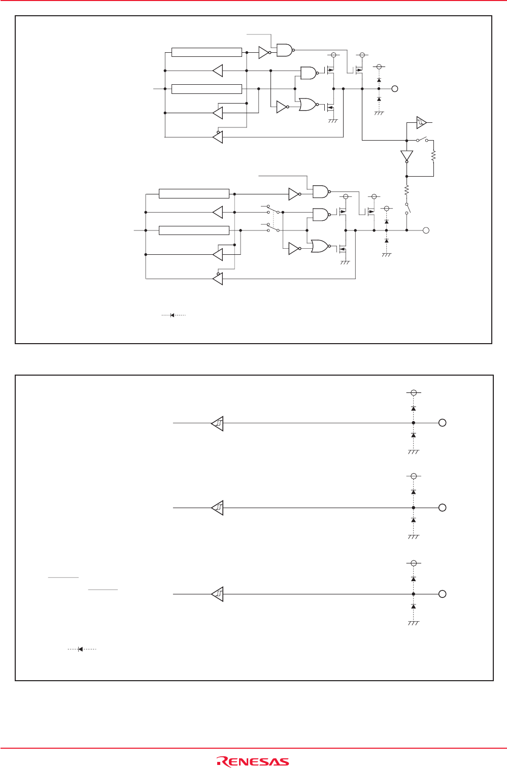
Figure19.5 I/O Ports (5)
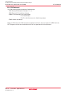
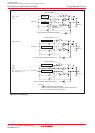
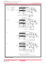
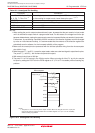
Figure19.6 I/O Pins
fC
Rf
Rd
Data bus
Direction register
Pull-up selection
Port latch
"1"
Output
Direction register
Pull-up selection
Port latch
Data bus
(NOTE 1)
(NOTE 1)
P8_7
P8_6
NOTE:
1. Symbolizes a parasitic diode.
Make sure the input voltage on each port will not exceed VCC.
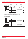
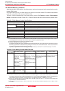
BYTE
BYTE signal input
CNVSS
CNVSS signal input
RESET
RESET signal input
(NOTE 1)
(NOTE 1)
(NOTE 1)
NOTE:
1. Symbolizes a parasitic diode.
Make sure the input voltage on each port will not exceed VCC.