


Rev.1.10 Jul 01, 2005 page 274 of 318
REJ09B0124-0110
M16C/6N Group (M16C/6NK, M16C/6NM) 21. Electric Characteristics
Under development
This document is under development and its contents are subject to change.
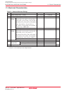
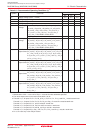
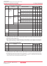
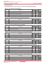
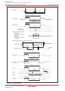
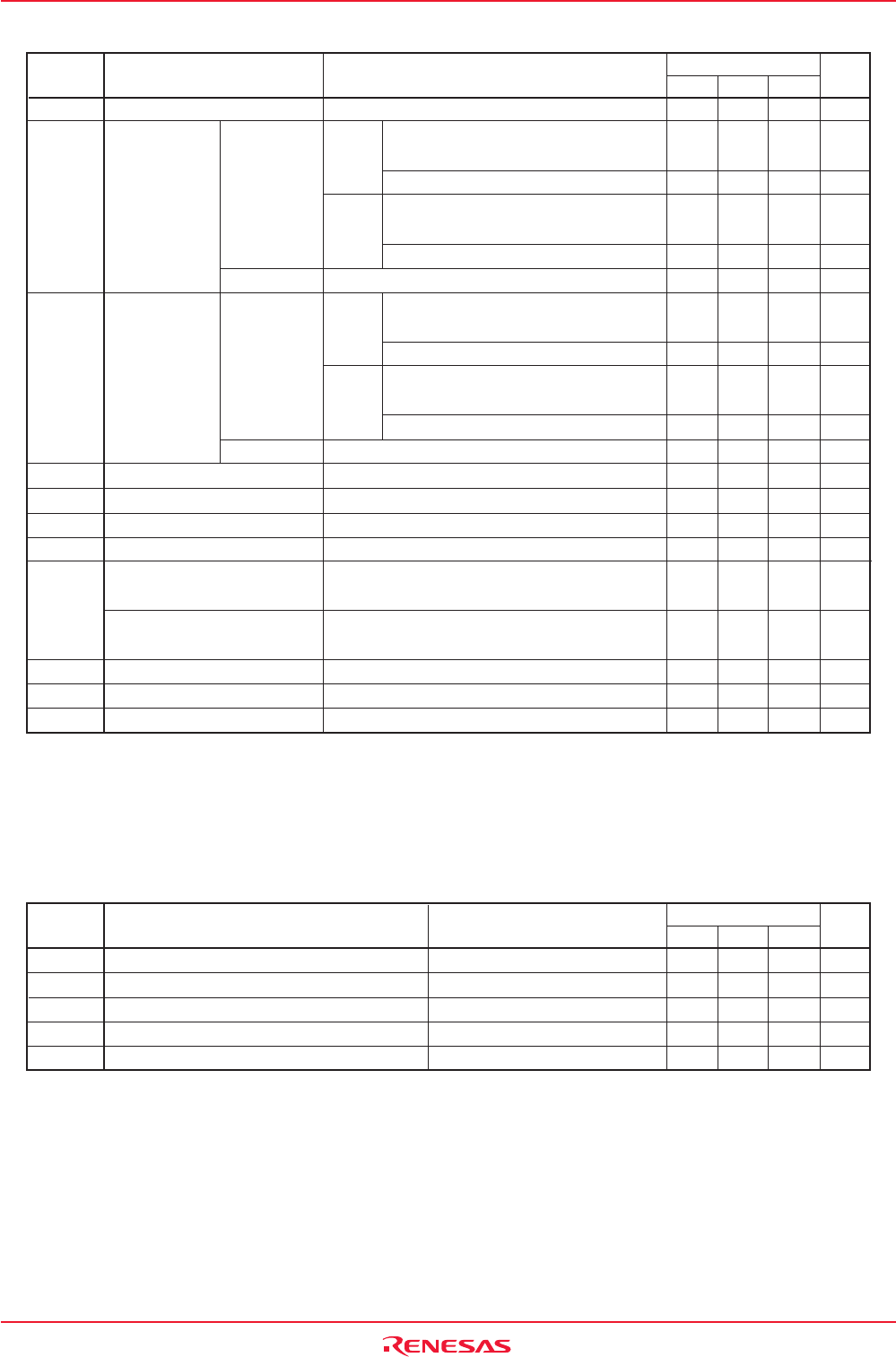
Table 21.6 A/D Conversion Characteristics
(1)
10
±3
±7
±5
±7
±2
±3
±7
±5
±7
±2
±1
±3
±3
40
V
CC
VREF
Bit
LSB
LSB
LSB
LSB
LSB
LSB
LSB
LSB
LSB
LSB
LSB
LSB
LSB
kΩ
µs
µs
µs
V
V
10
3.3
2.8
0.3
2.0
0
VREF = VCC
VREF
= VCC
= 5V
VREF
= VCC
= 3.3V
VREF = AVCC = VCC = 3.3V
VREF
= VCC
= 5V
VREF
= VCC
= 3.3V
VREF = AVCC = VCC = 3.3V
VREF = VCC
VREF = VCC = 5V, φAD = 10MHz
VREF = VCC = 5V, φAD = 10MHz
ANEX0, ANEX1 input, AN0 to AN7 input,
AN0_0 to AN0_7 input, AN2_0 to AN2_7 input
External operation amp connection mode
ANEX0, ANEX1 input, AN0 to AN7 input,
AN0_0 to AN0_7 input, AN2_0 to AN2_7 input
External operation amp connection mode
ANEX0, ANEX1 input, AN0 to AN7 input,
AN0_0 to AN0_7 input, AN2_0 to AN2_7 input
External operation amp connection mode
ANEX0, ANEX1 input, AN0 to AN7 input,
AN0_0 to AN0_7 input, AN2_0 to AN2_7 input
External operation amp connection mode
Resolution
Integral 10 bits
Nonlinearity
Error
8 bits
Absolute 10 bits
Accuracy
8 bits
Differential Nonlinearity Error
Offset Error
Gain Error
Resistor Ladder
10-bit Conversion Time,
Sample & Hold function Available
8-bit Conversion time,
Sample & Hold function Available
Sampling Time
Reference Voltage
Analog Input Voltage
–
INL
–
DNL
–
–
RLADDER
tCONV
tSAMP
VREF
VIA
Symbol Parameter
Min.
Standard
Unit
Measuring Condition
Max.
Typ.
(NOTE 2)
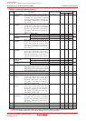
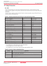
8
1.0
3
20
1.5
Bits
%
µs
kΩ
mA
Resolution
Absolute Accuracy
Setup Time
Output Resistance
Reference Power Supply Input Current
–
–
t
su
RO
IVREF
Symbol
Parameter
Min.
Standard
Unit
Measuring Condition
4
Max.Typ.
10
NOTES:
1. Referenced to VCC = AVCC = VREF = 3.3 to 5.5V, VSS = AVSS = 0V, –40 to 85°C unless otherwise specified.
2. φAD frequency must be 10MHz or less.
3. When sample & hold function is disabled, φAD frequency must be 250kHz or more in addition to a limit of NOTE 2.
When sample & hold function is enabled, φAD frequency must be 1MHz or more in addition to a limit of NOTE 2.
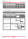
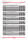
Table 21.7 D/A conversion Characteristics
(1)
NOTES:
1. Referenced to VCC = AVCC = VREF = 3.3 to 5.5V, VSS = AVSS = 0V, –40 to 85°C unless otherwise specified.
2. This applies when using one D/A converter, with the DAi register (i = 0, 1) for the unused D/A converter set to “00h”.
The resistor ladder of the A/D converter is not included. Also, the current I
VREF always flows even though VREF
may have been set to be unconnected by the ADCON1 register.