


Rev.1.10 Jul 01, 2005 page 8 of 318
REJ09B0124-0110
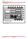
M16C/6N Group (M16C/6NK, M16C/6NM) 1. Overview
Under development
This document is under development and its contents are subject to change.
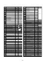
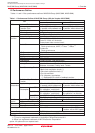
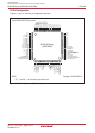
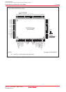
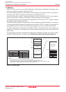
1.6 Pin Description
Tables 1.4 and 1.5 list the pin descriptions.
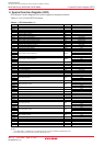
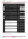
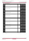
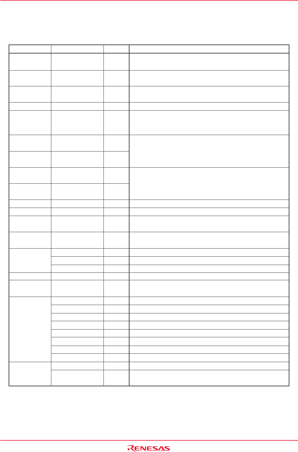
Table 1.4 Pin Description (100-pin and 128-pin Versions) (1)
I
I
I
I
I
I
O
I
O
O
I
I
I
I/O
I
I
I
O
I
O
I/O
I
I
O
O
O
I/O
I/O
VCC1, VCC2,
VSS
AVCC, AVSS
_____________
RESET
CNVSS
BYTE
XIN
XOUT
XCIN
XCOUT
CLKOUT
________ ________
INT0 to INT8
(3)
________
NMI
______ ______
KI0 to KI3
TA0OUT to TA4OUT
TA0IN to TA4IN
ZP
TB0IN to TB5IN
___ ___ ____
U, U, V, V, W, W
__________ __________
CTS0 to CTS2
__________ __________
RTS0 to RTS2
CLK0 to CLK6
(3)
RXD0 to RXD2
SIN3 to SIN6
(3)
TXD0 to TXD2
SOUT3 to SOUT6
(3)
CLKS1
SDA0 to SDA2
SCL0 to SCL2
Power supply
input
Analog power
supply input
Reset input
CNVSS
External data
bus width
select input
Main clock
input
Main clock
output
Sub clock
input
Sub clock
output
Clock output
______
INT interrupt input
_______
NMI interrupt
input
Key input
interrupt input
Timer A
Timer B
Three-phase motor
control output
Serial I/O
I
2
C mode
Apply 3.0 to 5.5V to the VCC1 and VCC2 pins and 0V to the
VSS pin. The VCC apply condition is that VCC2 = VCC1
(1)
.
Applies the power supply for the A/D converter. Connect the
AVCC pin to VCC1. Connect the AVSS pin to VSS.
The microcomputer is in a reset state when applying “L” to the
this pin.
Connect this pin to VSS.
Connect this pin to VSS.
I/O pins for the main clock oscillation circuit. Connect a ceramic
resonator or crystal oscillator between XIN and XOUT
(2)
.
To use the external clock, input the clock from XIN and leave
XOUT open.
I/O pins for a sub clock oscillation circuit. Connect a crystal
oscillator between XCIN and XCOUT
(2)
.
To use the external clock, input the clock from XCIN and leave
XCOUT open.
The clock of the same cycle as fC, f8, or f32 is output.
______
Input pins for the INT interrupt.
_______
Input pin for the NMI interrupt.
Input pins for the key input interrupt.
These are timer A0 to timer A4 I/O pins.
These are timer A0 to timer A4 input pins.
Input pin for the Z-phase.
These are timer B0 to timer B5 input pins.
These are Three-phase motor control output pins.
These are send control input pins.
These are receive control output pins.
These are transfer clock I/O pins.
These are serial data input pins.
These are serial data input pins.
These are serial data output pins.
These are serial data output pins.
This is output pin for transfer clock output from multiple pins function.
These are serial data I/O pins.
These are transfer clock I/O pins. (except SCL2 for the
N-channel open drain output.)
Signal Name Pin Name I/O Type Description
I: Input O: Output I/O: Input/Output
NOTES:
1. In this manual, hereafter, VCC refers to VCC1 unless otherwise noted.
2. Ask the oscillator maker the oscillation characteristic.
________ ________
3. INT6 to INT8, CLK5, CLK6, SIN5, SIN6, SOUT5, SOUT6 are only in the 128-pin version.