


Rev.1.10 Jul 01, 2005 page 216 of 318
REJ09B0124-0110
M16C/6N Group (M16C/6NK, M16C/6NM) 18. CAN Module
Under development
This document is under development and its contents are subject to change.
18.6 Configuration CAN Module System Clock
The M16C/6N Group (M16C/6NK, M16C/6NM) has a CAN module system clock select circuit.
Configuration of the CAN module system clock can be done through manipulating the CCLKR register and
the BRP bit in the CiCONR register (i = 0, 1).
For the CCLKR register, refer to 7. Clock Generating Circuit.
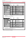
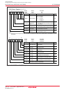
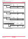
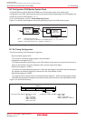
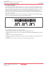
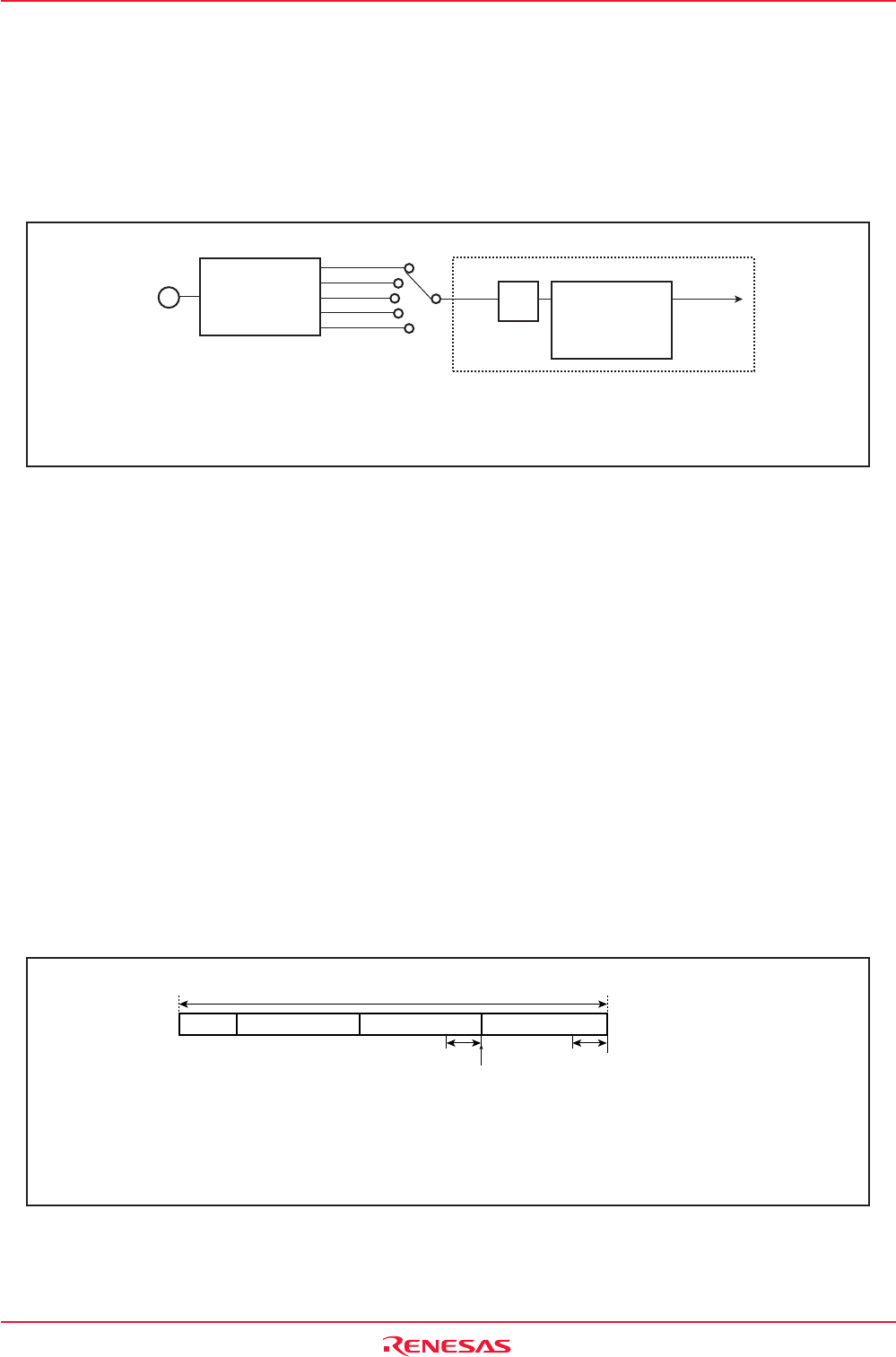
Figure 18.14 shows a block diagram of the clock generating circuit of the CAN module system.
Figure 18.14 Block Diagram of CAN Module System Clock Generating Circuit
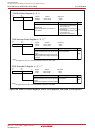
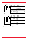
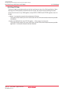
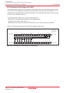
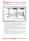
18.7 Bit Timing Configuration
The bit time consists of the following four segments:
• Synchronization segment (SS)
This serves for monitoring a falling edge for synchronization.
• Propagation time segment (PTS)
This segment absorbs physical delay on the CAN network which amounts to double the total sum of
delay on the CAN bus, the input comparator delay, and the output driver delay.
• Phase buffer segment 1 (PBS1)
This serves for compensating the phase error. When the falling edge of the bit falls later than expected,
the segment can become longer by the maximum of the value defined in SJW.
• Phase buffer segment 2 (PBS2)
This segment has the same function as the phase buffer segment 1. When the falling edge of the bit
falls earlier than expected, the segment can become shorter by the maximum of the value defined in SJW.
Figure 18.15 shows the bit timing.
Figure 18.15 Bit Timing
1/2
Divide-by-1
(undivided)
Divide-by-2
Divide-by-4
Divide-by-8
Divide-by-16
Prescaler
Baud rate
prescaler
division value
: P + 1
fCAN
fCANCLK
fCAN : CAN module system clock
P : The value written in the BRP bit in the CiCONR register ( i = 0, 1). P = 0 to 15
fCANCLK : CAN communication clock fCANCLK = fCAN/2(P + 1)
CAN module
system clock
divider
CCLKR register
Value: 1, 2, 4, 8, 16
CAN module
f1
The range of each segment: Bit time = 8 to 25Tq
SS = 1Tq
PTS = 1Tq to 8Tq
PBS1 = 2Tq to 8Tq
PBS2 = 2Tq to 8Tq
SJW = 1Tq to 4Tq
Configuration of PBS1 and PBS2: PBS1 ≥ PBS2
PBS1 ≥ SJW
PBS2 ≥ 2 when SJW = 1
PBS2 ≥ SJW when 2 ≤ SJW ≤ 4
Bit time
SS PTS PBS1
SJW
Sampling point
PBS2
SJW