


Rev.1.10 Jul 01, 2005 page 166 of 318
REJ09B0124-0110
M16C/6N Group (M16C/6NK, M16C/6NM) 14. Serial I/O
Under development
This document is under development and its contents are subject to change.
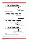
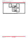
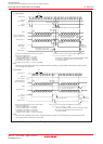
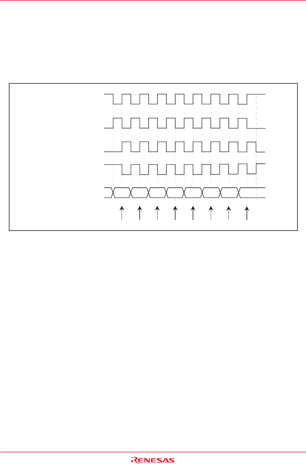
14.1.4.1 Clock Phase Setting Function
One of four combinations of transfer clock phases and polarities can be selected using the CKPH bit in
the UiSMR3 register and the CKPOL bit in the UiC0 register.
Make sure the transfer clock polarity and phase are the same for the master and salves to be communicated.
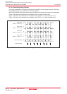
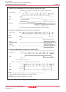
Figure 14.28 shows the transmission and reception timing in master (internal clock).
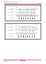
Figure 14.29 shows the transmission and reception timing (CKPH = 0) in slave (external clock).
Figure 14.30 shows the transmission and reception timing (CKPH = 1) in slave (external clock).
D0 D1 D2 D3 D4 D6 D7D5
"H"
"L"
"H"
"L"
"H"
"L"
"H"
"L"
"H"
"L"
Clock output
(CKPOL = 0, CKPH = 0)
Clock output
(CKPOL = 1, CKPH = 0)
Clock output
(CKPOL = 0, CKPH = 1)
Clock output
(CKPOL = 1, CKPH = 1)
Data output timing
Data input timing
Figure 14.28 Transmission and Reception Timing in Master Mode (Internal Clock)