


Rev.1.10 Jul 01, 2005 page 55 of 318
REJ09B0124-0110
M16C/6N Group (M16C/6NK, M16C/6NM) 7. Clock Generating Circuit
Under development
This document is under development and its contents are subject to change.
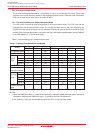
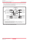
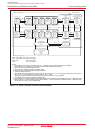
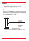
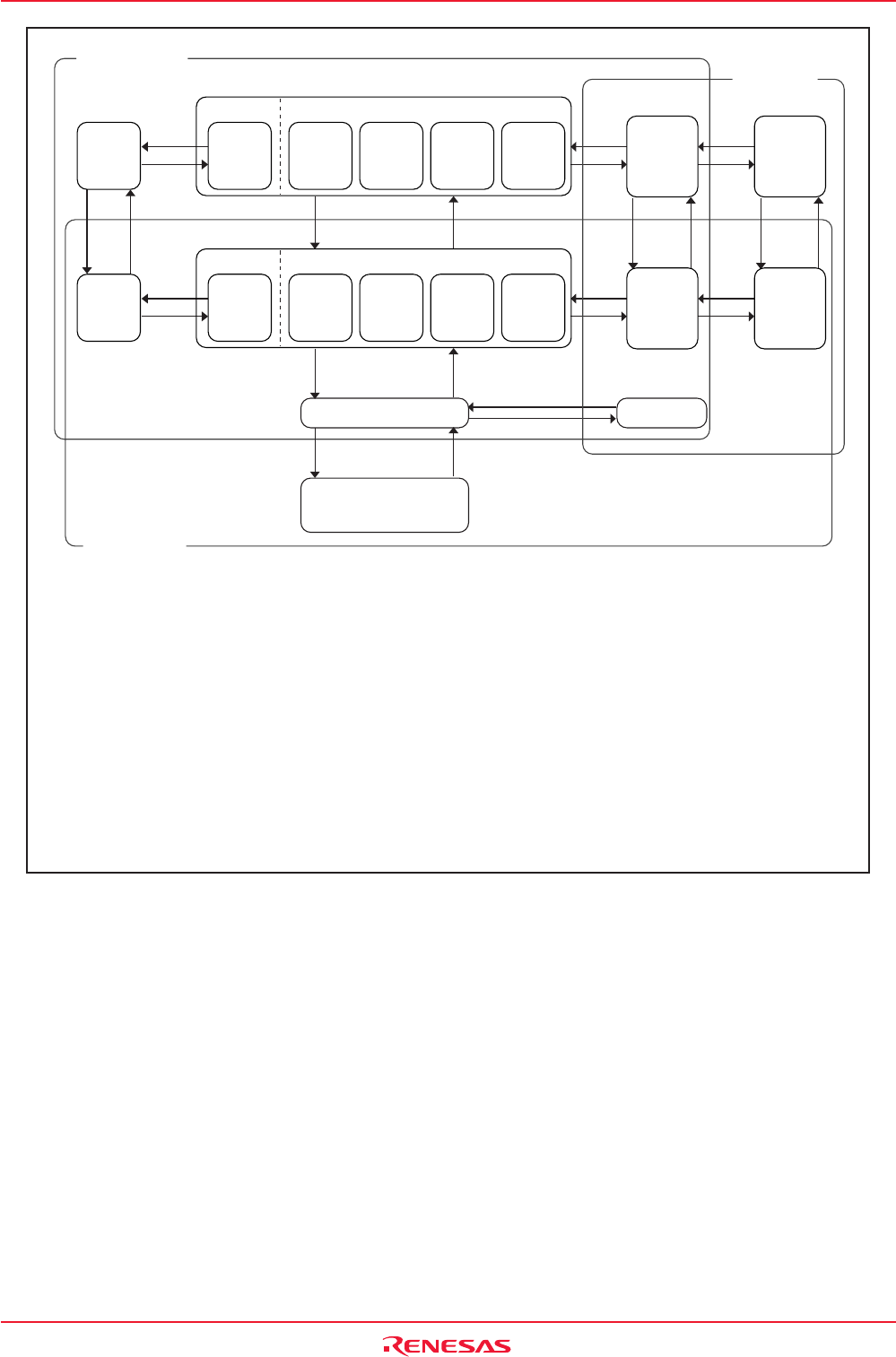
Figure 7.13 State Transition in Normal Operation Mode
CPU clock
: f(PLL)
CM07 = 0
CM06 = 0
CM17 = 0
CM16 = 0
PLL operation mode
PLL operation mode
PLC07 = 0
CM11 = 0
(7)
PLC07 = 1
CM11 = 1
(6)
CM04 = 1CM04 = 1 CM04 = 0 CM04 = 0
CM04 = 1
CM04 = 0
CM04 = 1
CM04 = 0
CM07 =1
(3)
CM07 = 0
(2) (4)
CPU clock
f(Ring)
f(Ring)/2
f(Ring)/4
f(Ring)/8
f(Ring)/16
On-chip Oscillator
Mode
CM21 = 1
CM21 = 0
(8)
High-Speed Mode
CPU clock
: f(XIN)
CM07 = 0
CM06 = 0
CM17 = 0
CM16 = 0
CPU clock
f(Ring)
f(Ring)/2
f(Ring)/4
f(Ring)/8
f(Ring)/16
On-chip Oscillator
Low Power Dissipation Mode
On-chip Oscillator
Mode
On-chip Oscillator
Low Power Dissipation Mode
On-chip Oscillator
Clock Oscillation
Main Clock Oscillation
CM05 = 1
(1)
CM05 = 0
CM04, CM05, CM06, CM07: Bits in CM0 register
CM11, CM15, CM16, CM17: Bits in CM1 register
CM20, CM21 : Bits in CM2 register
PLC07 : Bit in PLC0 register
NOTES:
1. Avoid making a transition when the CM20 bit is set to "1" (oscillation stop, re-oscillation detection function enabled).
Set the CM20 bit to "0" (oscillation stop, re-oscillation detection function disabled) before transiting.
2. Wait for the main clock oscillation stabilization time.
3. Switch clock after oscillation of sub clock is sufficiently stable.
4. Change the CM17 and CM16 bits before changing the CM06 bit.
5. Transit in accordance with arrow.
6. The PM20 bit in the PM2 register become effective when the PLC07 bit is set to "1" (PLL on). Change the PM20 bit when the PLC07 bit is
set to "0" (PLL off). Set the PM20 bit to "0" (2 waits) when PLL clock > 16 MHz.
PM20 bit to "0" (SFR accessed with two wait states) before setting the PLC07 bit to "1" (PLL operation).
7. PLL operation mode can only be changed to high-speed mode.
8. Set the CM06 bit to "1" (division by 8 mode) before changing back the operation mode from on-chip oscillator mode to high- or middle-speed mode.
9. When the CM21 bit = 0 (on-chip oscillator turned off) and the CM05 bit = 1 (main clock turned off), the CM06 bit is fixed to "1" (divide-by-8 mode)
and the CM15 bit is fixed to "1" (drive capability High).
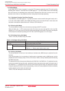
Medium-Speed Mode
(divide by 2)
CPU clock
: f(XIN)/2
CM07 = 0
CM06 = 0
CM17 = 0
CM16 = 1
Medium-Speed Mode
(divide by 4)
CPU clock
: f(XIN)/4
CM07 = 0
CM06 = 0
CM17 = 1
CM16 = 0
Medium-Speed Mode
(divide by 8)
CPU clock
: f(XIN)/8
CM07 = 0
CM06 = 1
Medium-Speed Mode
(divide by 16)
CPU clock
: f(XIN)/16
CM07 = 0
CM06 = 0
CM17 = 1
CM16 = 1
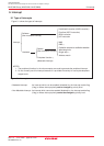
CPU clock
: f(PLL)
CM07 = 0
CM06 = 0
CM17 = 0
CM16 = 0
PLC07 = 0
CM11 = 0
(7)
PLC07 = 1
CM11 = 1
(6)
CPU clock
f(Ring)
f(Ring)/2
f(Ring)/4
f(Ring)/8
f(Ring)/16
CM21 = 1
CM21 = 0
(8)
CM21 = 1
CM21 = 0
High-Speed mode
CPU clock
: f(XIN)
CM07 = 0
CM06 = 0
CM17 = 0
CM16 = 0
CPU clock
f(Ring)
f(Ring)/2
f(Ring)/4
f(Ring)/8
f(Ring)/16
Sub clock oscillation
CM05 = 1
(1)
CM05 = 0
Medium-Speed Mode
(divide by 2)
CPU clock
: f(XIN)/2
CM07 = 0
CM06 = 0
CM17 = 0
CM16 = 1
Medium-Speed Mode
(divide by 4)
CPU clock
: f(XIN)/4
CM07 = 0
CM06 = 0
CM17 = 1
CM16 = 0
Medium-Speed Mode
(divide by 8)
CPU clock
: f(XIN)/8
CM07 = 0
CM06 = 1
Medium-Speed Mode
(divide by 16)
CPU clock
: f(XIN)/16
CM07 = 0
CM06 = 0
CM17 = 1
CM16 = 1
CPU clock: f(XCIN)
CM07 = 0
CPU clock: f(XCIN)
CM07 = 0
Low-Speed ModeLow-Speed Mode
CM05 = 1
(1) (9)
CM05 = 0
CPU clock: f(XCIN)
CM07 = 0
CM06 = 1
CM15 = 1
Low Power Dissipation Mode