


Rev.1.10 Jul 01, 2005 page 9 of 318
REJ09B0124-0110
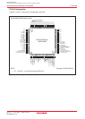
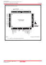
M16C/6N Group (M16C/6NK, M16C/6NM) 1. Overview
Under development
This document is under development and its contents are subject to change.
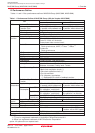
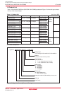
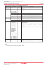
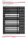
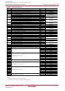
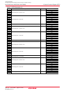
Table 1.5 Pin Description (100-pin and 128-pin Versions) (2)
Applies the reference voltage for the A/D converter and D/A
converter.
Analog input pins for the A/D converter.
This is an A/D trigger input pin.
This is the extended analog input pin for the A/D converter,
and is the output in external op-amp connection mode.
This is the extended analog input pin for the A/D converter.
These are the output pins for the D/A converter.
These are the input pins for the CAN module.
These are the output pins for the CAN module.
8-bit I/O ports in CMOS, having a direction register to select
an input or output.
Each pin is set as an input port or output port. An input port
can be set for a pull-up or for no pull-up in 4-bit unit by
program.
(except P7_1 and P9_1 for the N-channel open drain output.)
_______
Input pin for the NMI interrupt.
Pin states can be read by the P8_5 bit in the P8 register.
Reference
voltage input
A/D converter
D/A converter
CAN module
I/O port
Input port
VREF
AN0 to AN7
AN0_0 to AN0_7
AN2_0 to AN2_7
_____________
ADTRG
ANEX0
ANEX1
DA0, DA1
CRX0, CRX1
CTX0, CTX1
P0_0 to P0_7
P1_0 to P1_7
P2_0 to P2_7
P3_0 to P3_7
P4_0
to
P4_7
P5_0 to P5_7
P6_0 to P6_7
P7_0 to P7_7
P8_0 to P8_4
P8_6, P8_7
P9_0 to P9_7
P10_0 to P10_7
P11_0 to P11_7
(1)
P12_0 to P12_7
(1)
P13_0 to P13_7
(1)
P14_0, P14_1
(1)
P8_5
I
I
I
I/O
I
O
I
O
I/O
I
Signal Name Pin Name I/O Type Description
I: Input O: Output I/O: Input/Output
NOTE:
1. Ports P11 to P14 are only in the 128-pin version.