


Rev.1.10 Jul 01, 2005 page 37 of 318
REJ09B0124-0110
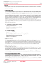
M16C/6N Group (M16C/6NK, M16C/6NM) 7. Clock Generating Circuit
Under development
This document is under development and its contents are subject to change.
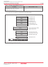
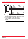
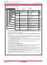
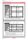
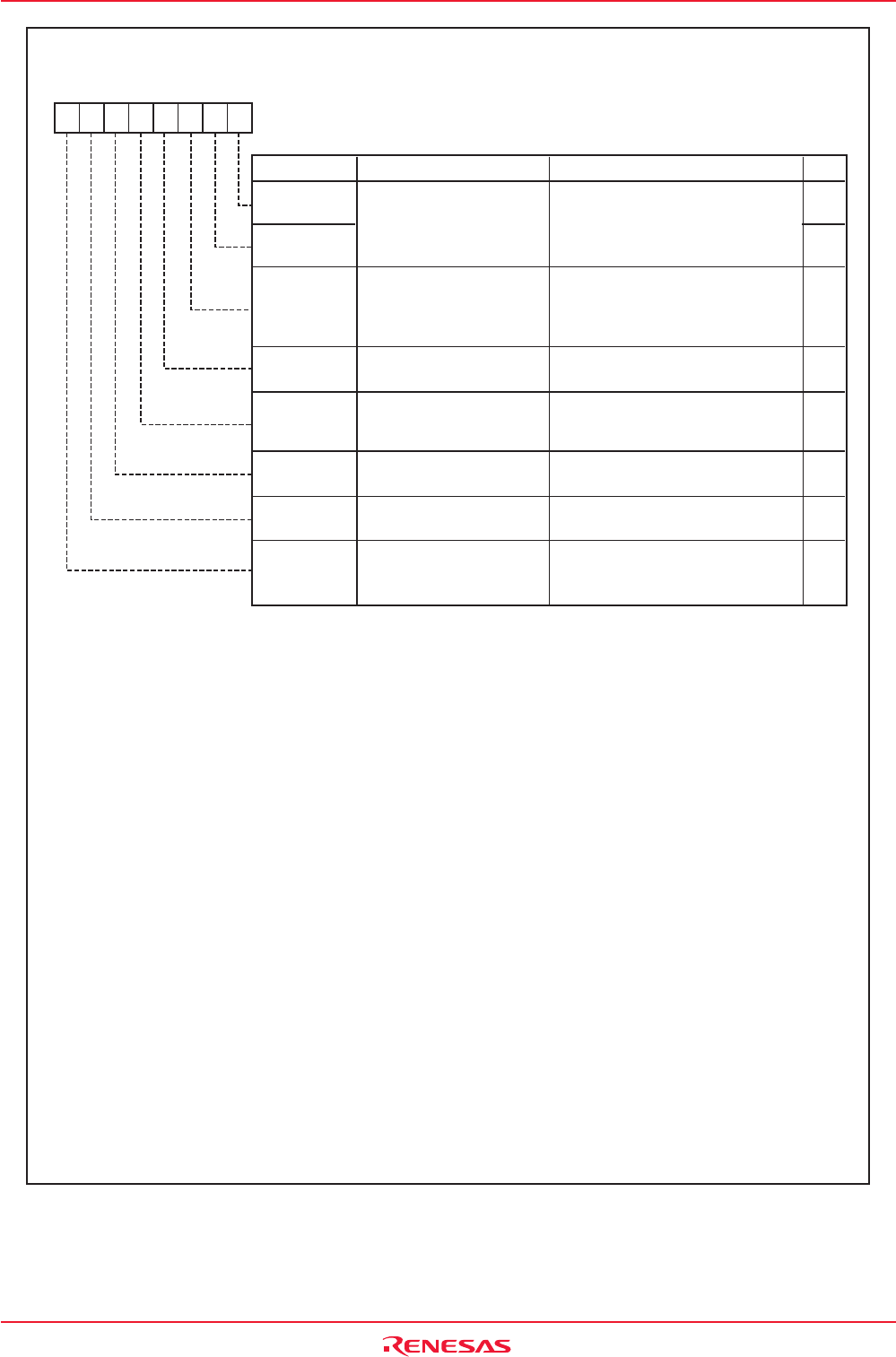
Figure 7.2 CM0 Register
System Clock Control Register 0
(1)
NOTES:
1. Write to this register after setting the PRC0 bit in the PRCR register to "1" (write enable).
2. The fC32 clock does not stop. During low-speed or low power dissipation mode, do not set this bit to "1"
(peripheral clock turned off when in wait mode).
3. The CM03 bit is set to "1" (high) while the CM04 bit is set to "0" (I/O port) or when entered to stop mode.
4. To use a sub clock, set this bit to "1". Also make sure ports P8_6 and P8_7 are directed for input, with no
pull-ups.
5. This bit is provided to stop the main clock when the low power dissipation mode or on-chip oscillator low
power dissipation mode is selected. This bit cannot be used for detection as to whether the main clock stopped
or not. To stop the main clock, set bits in the following order.
(1) Set the CM07 bit to "1" (sub clock select) or the CM21 bit in the CM2 register to "1" (on-chip oscillator select)
with the sub clock stably oscillating.
(2) Set the CM20 bit in the CM2 register to "0" (oscillation stop, re-oscillation detection function disabled).
(3) Set the CM05 bit to "1" (stop).
6. To use the main clock as the clock source for the CPU clock, set bits in the following order.
(1) Set the CM05 bit to "0" (oscillate)
(2) Wait until the main clock oscillation stabilizes.
(3) Set the CM11, CM21 and CM07 bits all to "0".
7. When the CM21 bit = 0 (on-chip oscillator turned off) and the CM05 bit = 1 (main clock turned off), the CM06
bit is fixed to "1" (divide-by-8 mode) and the CM15 bit is fixed to "1" (drive capability High).
8. During external clock input, set the CM05 bit to "0" (oscillate).
9. When the CM05 bit is set to "1", the XOUT pin goes "H". Furthermore, because the internal feedback resistor
remains connected, the XIN pin is pulled "H" to the same level as XOUT via the feedback resistor.
10. When entering stop mode from high- or medium-speed mode, on-chip oscillator mode or on-chip oscillator
low power dissipation mode, the CM06 bit is set to "1" (divide-by-8 mode).
11. After setting the CM04 bit to "1" (XCIN-XCOUT oscillator function), wait until the sub clock oscillates stably
before switching the CM07 bit from "0" to "1" (sub clock).
12. To return from on-chip oscillator mode to high-speed or medium-speed mode, set the CM06 and CM15 bits
both to "1".
Bit Name FunctionBit Symbol
b1 b0
RW
RW
RW
RW
RW
RW
RW
RW
RW
0 0 : I/O port P5_7
0 1 : fC output
1 0 : f8 output
1 1 : f32 output
0 : Do not stop peripheral function
clock in wait mode
1 : Stop peripheral function clock
in wait mode
(2)
0 : I/O port P8_6, P8_7
1 : XCIN-XCOUT generation
function
(4)
0 : On
1 : Off
(8) (9)
0 : CM16 and CM17 valid
1 : Division by 8 mode
0 : Main clock, PLL clock,
or on-chip oscillator clock
1 : Sub clock
0 : LOW
1 : HIGH
CM07
CM05
CM04
CM01
CM02
CM00
CM06
Clock Output Function
Select Bit
(Valid only in single-chip
mode)
CM03
WAIT Mode Peripheral
Function Clock Stop Bit
Port XC Select Bit
(3)
Main Clock Stop Bit
(5) (6) (7)
Main Clock Division Select
Bit 0
(7) (10) (12)
XCIN-XCOUT Drive
Capacity Select Bit
(3)
System Clock Select
Bit
(6) (11)
Symbol Address After Reset
CM0 0006h 01001000b
b7 b6 b5 b4 b3 b2 b1 b0