


Rev.1.10 Jul 01, 2005 page 40 of 318
REJ09B0124-0110
M16C/6N Group (M16C/6NK, M16C/6NM) 7. Clock Generating Circuit
Under development
This document is under development and its contents are subject to change.
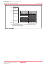
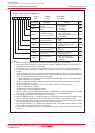
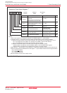
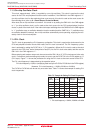
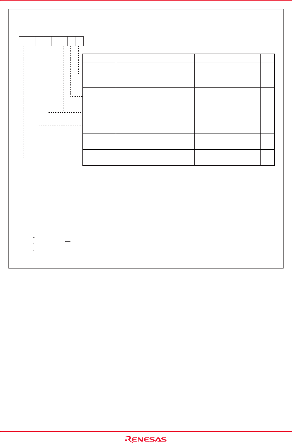
Figure 7.5 PCLKR Register
NOTES:
1. Write to this register after setting the PRC0 bit in the PRCR register to "1" (write enable).
2. If this bit is set to "1", the software interrupt number and SFR location can be changed as follows.
(1) Software interrupt number of the key input interrupt in the vector table can be changed from 14 to 13.
- No.13 is changed from the CAN0/1 error interrupt to the CAN0/1 error/key input interrupt.
- No.14 is changed from the A/D/key input interrupt to the A/D interrupt.
(2) Address of the KUPIC register in the SFR can be changed from 004Eh to 004Dh.
- Address 004Dh is changed from the C01ERRIC register to the C01ERRIC/KUPIC register.
- Address 004Eh is changed from the ADIC/KUPIC register to the ADIC register.
3. When this bit = 1, the A/D clock is set to divide-by-1 of fAD mode regardless of whether the PCLK0 bit is set.
4. When the PCLK5 bit and the SM43 bit in the S4C register = 1, the pin function of SI/O4 can be changed as follows.
P8_0/TA4OUT/U/(SIN4)
P7_5/TA2IN/W/(SOUT4)
P7_4/TA2OUT/W/(CLK4)
5. SI/O5 and SI/O6 are only in the 128-pin version.
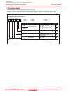
Peripheral Clock Select Register
(1)
Symbol Address After Reset
PCLKR 025Eh 00h
000
b7 b6 b5 b4 b3 b2 b1 b0
PCLK0
PCLK1
-
(b4-b2)
SI/O Clock Select Bit
(Clock source for UART0 to UART2,
SI/O3 to SI/O6)
(5)
0 : Divide-by-2 of fAD, f2
1 : fAD, f1
0 : f2SIO
1 : f1SIO
Reserved Bit
Set to "0"
RW
RW
RW
RW
RW
RW
Bit Name FunctionBit Symbol
RW
Timers A, B, and A/D Clock
Select Bit
(Clock source for the timers A, B,
the dead time timer and A/D)
Pin Function Swirch Bit
0: Normal mode
1: Swiching mode
(4)
PCLK5
Software Interrupt Number/SFR
Location Switch Bit
0: Normal mode
1: Swiching mode
(2)
PCLK6
A/D Clock Direct Input Bit
0: Normal mode
1: Swiching mode
(3)
PCLK7